
Technical Resources
ZnSe Lens Manufacturer: Grades, Tolerances & Coatings
Choosing a ZnSe lens manufacturer comes down to three things you can actually verify: the grade and traceability of the chemical vapor deposition (CVD) zinc selenide blank, the measured bulk absorption at your operating wavelength, and whether the polishing and coating processes hold surface figure and damage threshold under thermal load. Diameter, focal length, and a single transmission number tell you very little, because two lenses with identical geometry and identical quoted transmission can behave completely differently in a 4 kW cutting head.
This article covers the physics that drives those differences, the parameters that belong on your drawing, and the questions that separate a component supplier from a company that understands your system.
Why ZnSe dominates CO2 laser and LWIR optics
Zinc selenide transmits from roughly 0.6 to 21 microns, which makes it one of the few materials that covers the 10.6 micron CO2 laser line, the 8 to 12 micron long-wave infrared (LWIR) imaging band, and the visible red at the same time. That last point is practical rather than cosmetic: a ZnSe optic passes a HeNe alignment beam, so you can align an invisible CO2 beam path with visible light through the same optics.
The reason it wins at high power is bulk absorption. Laser-grade CVD ZnSe is typically specified at an absorption coefficient of 0.0005 cm-1 or lower at 10.6 microns, which is roughly one to two orders of magnitude below gallium arsenide (GaAs) and multispectral zinc sulfide (ZnS). Less absorbed power means less heat deposited in the lens, and heat in the lens is what moves your focus.
The penalty is refractive index. ZnSe has an index of about 2.4028 at 10.6 microns, so the Fresnel reflection at each uncoated surface is:
R = ((n – 1) / (n + 1))2 = (1.4028 / 3.4028)2 ≈ 0.17
That is about 17 percent per surface and roughly 29 percent through a two-surface element. An uncoated ZnSe lens is not a usable laser optic. The antireflection (AR) coating is not an upgrade on a ZnSe lens, it is a functional requirement, and coating quality is therefore a large part of what you are buying from any ZnSe lens manufacturer.
Material grades: what “CVD ZnSe” actually leaves unsaid
Nearly all optical ZnSe is polycrystalline material grown by chemical vapor deposition from zinc vapor and hydrogen selenide. Single-crystal ZnSe exists and shows lower absorption, but it is rare and expensive in the sizes used for laser optics.
Within CVD material, suppliers separate at least two grades:
- Standard or optical grade. Suitable for thermal imaging, spectroscopy windows, ATR elements, and low-power beam delivery. Absorption is not individually certified.
- Laser grade. Material selected or post-processed for low absorption and low scatter, intended for kilowatt-class CO2 systems. Absorption is measured, usually by laser calorimetry.
The distinction matters because transmission measured on a spectrophotometer cannot separate absorption from scatter. A lens can measure 99.5 percent transmission and still deposit unacceptable heat in the bulk. If your application is above a few hundred watts, ask for the calorimetric absorption value, not the transmission curve.
Polishing versus single-point diamond turning
ZnSe is soft, with a Knoop hardness around 120 kg/mm2, which makes it well suited to single-point diamond turning (SPDT). SPDT is the practical route for aspheres, off-axis geometries, and diffractive surfaces that cannot be conventionally polished. The trade-off is residual periodic tool marks, which raise scatter and can lower damage threshold. For high-power spherical CO2 optics, conventional polishing or post-turning polishing is generally preferred. For a molded or diamond-turned LWIR asphere in an imaging system, the tool marks are usually irrelevant.
Material comparison for the 8 to 12 micron band
ZnSe is the default, not the only answer. In dirty, high-spatter environments, its softness becomes the limiting factor, and a harder material may survive longer even though it absorbs more.
| Property (typical published values) | ZnSe | ZnS (multispectral) | GaAs | Germanium |
|---|---|---|---|---|
| Useful transmission range (µm) | 0.6 to 21 | 0.4 to 12 | 1 to 15 | 2 to 14 |
| Refractive index at 10.6 µm | 2.40 | 2.20 | 3.28 | 4.00 |
| Bulk absorption at 10.6 µm (cm-1) | ≤0.0005 (laser grade) | ~0.2 (standard ZnS) | ~0.01 | ~0.02 to 0.03 |
| Knoop hardness (kg/mm2) | ~120 | ~150 to 230 | ~750 | ~780 |
| dn/dT at 10.6 µm (10-6 K-1) | ~+61 | ~+41 | ~+150 | ~+400 |
| Visible transparency for alignment | Yes (red) | Yes | No | No |
| Best fit | High-power CO2, multispectral | Vis to LWIR imaging, harsh windows | CO2 in spatter-heavy cutting | Passive LWIR imaging |
Germanium deserves one warning that catches people out: its very large dn/dT and its absorption both climb steeply with temperature, so a germanium element in a beam path can enter thermal runaway. ZnSe does not behave that way at comparable power levels, which is exactly why it remains the standard for transmissive CO2 optics.
What belongs on a ZnSe lens drawing
The following are industry-typical commercial values. Any manufacturer can tighten them, and every tightening costs money and yield, so specify what your system needs rather than the tightest number on the page.
| Parameter | Economy | Typical commercial | Precision |
|---|---|---|---|
| Diameter tolerance | +0 / -0.15 mm | +0 / -0.10 mm | +0 / -0.025 mm |
| Center thickness tolerance | ±0.20 mm | ±0.10 mm | ±0.05 mm |
| Focal length tolerance | ±3% | ±2% | ±1% |
| Surface quality (MIL-PRF-13830B scratch-dig) | 80-50 | 40-20 | 20-10 |
| Surface figure at 632.8 nm | λ/2 P-V | λ/4 P-V | λ/10 P-V |
| Centration / wedge | 5 arcmin | 3 arcmin | <1 arcmin |
| Clear aperture | 85% of diameter | 90% | 95% |
| AR coating reflectance per surface | R < 0.5% at 10.6 µm | R < 0.2% at 10.6 µm | Application specific |
Two notes on the table. First, surface figure on ZnSe is normally measured with a visible interferometer at 632.8 nm because the material transmits red, unlike germanium or silicon, which require an infrared interferometer. That difference shows up in test cost and in how quickly a supplier can give you real interferograms. Second, MIL-PRF-13830B scratch-dig is a visual comparison method and is interpreted differently between vendors. If cosmetic defects genuinely affect your system, specify ISO 10110-7 surface imperfection tolerances instead, which are dimensional and measurable.
For coatings, decide early whether you need a narrowband AR centered on your laser line or a broadband 8 to 12 micron AR for imaging. A single-wavelength design will always beat a broadband design at that wavelength. Suppliers of infrared lenses and custom optical coatings, including GIAI Photonics, generally treat the AR design as part of the component specification rather than a catalog add-on, and that is the correct way to buy it.
Thermal lensing: the trade-off that decides real systems
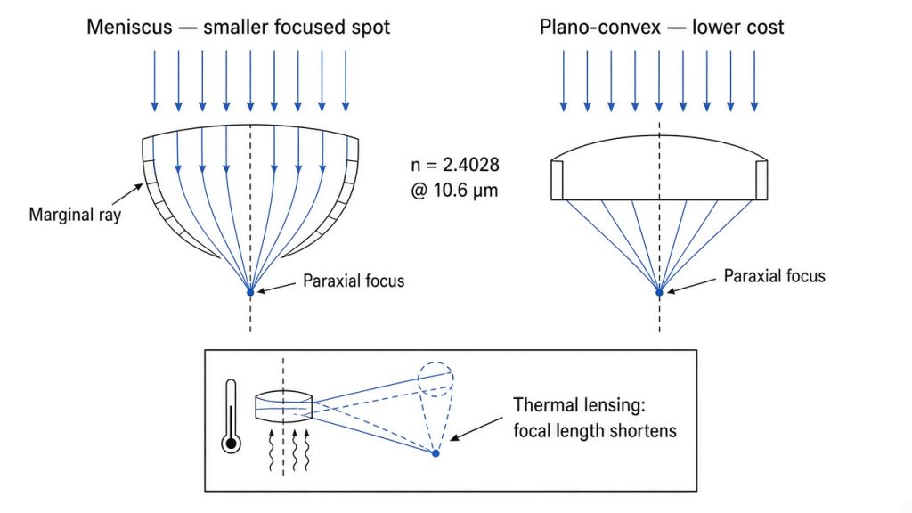
Every watt absorbed in the lens does two things: it expands the glass and it raises the refractive index, since dn/dT for ZnSe is positive at about +61 x 10-6 K-1. Both effects shorten the focal length. This is thermal lensing, and it is why a cutting head that is dialed in on the first part can drift by the tenth part.
The magnitude is easy to bound. Bulk absorbed power is approximately:
Pabs ≈ Pin · α · L
For a 4 kW beam through a 10 mm thick laser-grade lens with α = 0.0005 cm-1, the bulk absorbs roughly 2 W. The AR coatings typically absorb more than the bulk does, and a standard AR coating is commonly quoted as absorbing under 0.2 percent of incident power, which puts another several watts into two thin films. A fingerprint or a film of oil on the surface can dwarf both.
Three practical consequences follow. Absorption specification matters more than transmission specification at high power. Coating absorption, not bulk absorption, is often the dominant term, so ask how the coating is deposited and how it is cleaned. And a lens that is running hot enough to shift focus is also running hot enough to accelerate coating failure, so focus drift is an early warning, not a nuisance.
Meniscus or plano-convex
Positive meniscus lenses reduce spherical aberration relative to plano-convex lenses and therefore produce a smaller focused spot, with the advantage growing as focal length shortens and beam diameter grows. Plano-convex lenses are cheaper to make and perfectly adequate at long focal lengths and high f-numbers. In a cutting head the lens also seals the assist-gas pressure region, so edge thickness has to be specified against the working pressure, and high-pressure designs use thicker elements. Thicker elements absorb slightly more, which is a real, if small, trade against mechanical safety.
What to ask a ZnSe lens manufacturer
These questions separate suppliers who control their process from suppliers who resell blanks:
- Is the material laser grade, and can you provide the measured absorption coefficient for this batch rather than a datasheet value?
- Is the AR coating designed for my exact wavelength, and what is the reflectance per surface at that wavelength and at my angle of incidence?
- What is the laser-induced damage threshold, and under what test conditions was it measured (wavelength, pulse duration or CW, spot size, number of shots)?
- Do you polish, diamond-turn, or both, and which was used for this part?
- Can you supply interferograms and a coating transmission scan with the shipment?
- How is the part cleaned and packaged, and what is the recommended field cleaning procedure?
- Is there a documented handling and disposal procedure for selenide dust and broken parts?
The last one is not paperwork. Zinc selenide is toxic, and grinding, polishing, or breaking it generates hazardous dust. A manufacturer that cannot answer that question is telling you something about the rest of its process control.
Common specification mistakes
Ordering a 10.6 micron lens for a 9.3 micron laser. Sealed-tube and RF-excited CO2 lasers also run on the 9.3 micron line for PET film, polyimide, and PCB work. The bulk material is fine at both wavelengths, but an AR coating optimized for 10.6 microns can show significantly higher reflectance at 9.3 microns. The result is lost power, higher coating absorption, and back reflection toward the resonator. Always state the wavelength on the purchase order, not just “CO2”.
Specifying transmission when you mean absorption. Covered above, and it is the single most common source of unexplained thermal drift.
Installing the lens backwards. For a plano-convex focusing lens the convex surface faces the collimated beam. Reversed, spherical aberration rises sharply and the spot grows. Meniscus lenses have a defined orientation as well, and an unmarked lens in a service kit is an incident waiting to happen. Ask for orientation marking on the mount edge or the packaging.
Cleaning ZnSe like glass. At Knoop 120 it scratches under pressure that a BK7 window would ignore. Dry wiping drags particulate across a soft coated surface. Use the drop-and-drag method with spectroscopic-grade solvent, handle with gloves or finger cots, and treat a scratched lens as consumed rather than repairable.
Assuming a clear aperture equals the diameter. With a 90 percent clear aperture on a 25 mm lens, the outer 1.25 mm annulus is not guaranteed. If your beam plus alignment tolerance fills the aperture, specify a larger diameter rather than hoping the edge performs.
FAQ
What is the difference between laser-grade and standard CVD ZnSe?
Both are polycrystalline CVD material. Laser grade is selected or further processed for low bulk absorption and low scatter, and its absorption coefficient is measured, usually by calorimetry, rather than assumed. For continuous-wave power above a few hundred watts, the difference shows up as focus stability and coating lifetime. Below that level, standard grade is often adequate and noticeably cheaper.
Can I use a 10.6 micron lens on a 9.3 micron laser?
The substrate transmits both wavelengths, so it will pass light. The problem is the coating. An AR design centered at 10.6 microns is not optimized at 9.3 microns, so reflectance per surface rises, more power is deposited in the film, and reflected power heads back up the beam path. Order the coating for your wavelength, or specify a dual-band AR if the system runs both.
Why does my focus position drift after a few minutes of operation?
Almost always thermal lensing. Absorbed power heats the lens, the surface curvature changes, and the refractive index rises because dn/dT is positive, all of which shorten the focal length. Contamination on the lens surface is the most common accelerator. Check surface cleanliness first, then the coating absorption, then the material grade.
Should I specify MIL-PRF-13830B or ISO 10110?
MIL-PRF-13830B scratch-dig is common in North America and is quick to quote, but it is a visual comparison against reference standards and interpretation varies between vendors. ISO 10110-7 defines imperfections dimensionally and is verifiable. If cosmetic defects affect scatter or damage threshold in your system, specify ISO 10110 and accept the higher inspection cost.
Is ZnSe dangerous to handle?
Intact, coated optics are safe to handle with gloves or finger cots. The hazard is selenium-containing dust generated by grinding, polishing, or breakage, and the residue from cleaning. Do not machine ZnSe without local exhaust ventilation, do not dispose of broken parts in general waste, and follow the supplier safety data sheet for your jurisdiction.
Meniscus or plano-convex for a cutting head?
Meniscus for short focal lengths and large input beams, where reduced spherical aberration gives a measurably smaller spot. Plano-convex for long focal lengths and high f-numbers, where the optical difference is small and the cost difference is not. Also confirm the edge thickness is rated for your assist-gas pressure.
Specifying with a supplier
If you are scoping a ZnSe focusing lens, window, or a custom infrared coating design, GIAI Photonics can review the wavelength, power, and aperture requirements against its infrared lens and optical coating capabilities.