
- Judge a germanium lens supplier on infrared metrology capability, not on polishing capability alone.
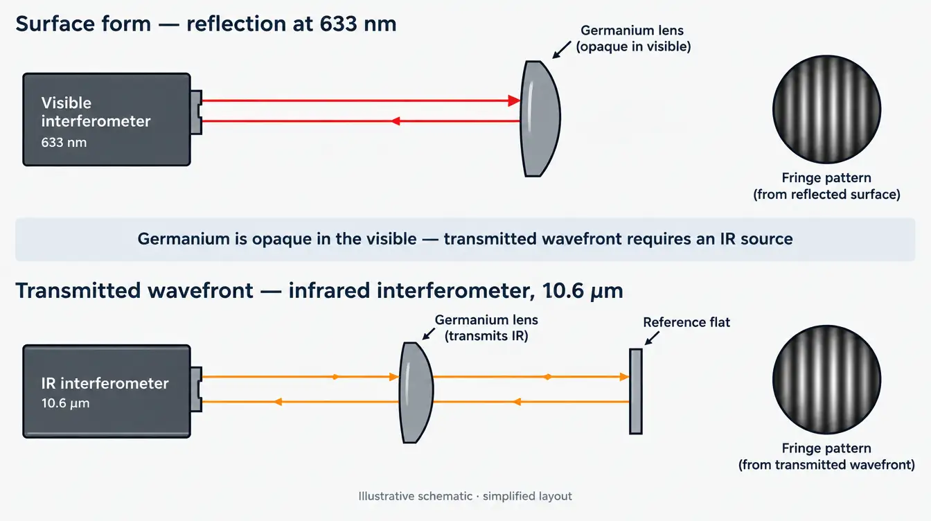
- Germanium is opaque in the visible, so transmitted wavefront must be measured at infrared wavelengths.
- Every fringe specification is meaningless without its test wavelength stated on the drawing.
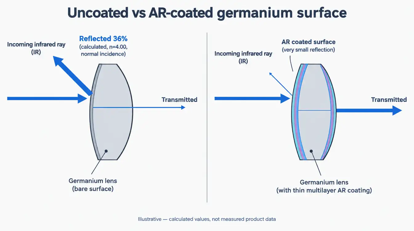
- Uncoated germanium reflects a large fraction per surface because its refractive index is near 4.
- Specify substrate resistivity and crystal form, not just the word “germanium”.
A germanium lens manufacturer should be judged on four things: control of the germanium substrate, the figuring route used to generate the surfaces, the infrared coating process, and the ability to measure the finished part at infrared wavelengths. Many visible-light optical shops can cut and polish germanium. Fewer can verify it. Acceptance disputes tend to start in that gap.
Germanium behaves unlike any glass an optical shop normally handles. It is opaque to the eye, its refractive index is close to 4, its absorption rises with temperature, and its surface tolerances are referenced to wavelengths roughly seventeen times longer than the visible ones most metrology labs are built around. Those four facts drive almost every sourcing decision below.
Why does germanium need a different manufacturing route than glass?
Germanium is a crystalline semiconductor with a band gap near 0.67 eV, which places its short-wavelength cut-on close to 1.8 µm. Below that, it absorbs; above it, the material transmits through the mid-wave and long-wave infrared until multiphonon lattice absorption takes over through the 14–16 µm region. The practical working window quoted for optical-grade germanium is 2–14 µm.
The high refractive index is the second driver. Taking n = 4.00 near 10 µm, the Fresnel reflectance at a single air–germanium interface at normal incidence is R = ((4.00 − 1)/(4.00 + 1))² = 0.36, or 36%. For a plane-parallel uncoated part, ignoring absorption and ignoring multiple internal reflections, two surfaces leave 0.64² = 41% transmission; accounting for incoherent multiple reflections in a non-absorbing slab, the figure is 2n/(n² + 1) = 47%. These are calculated values under the stated assumptions, not measured product data. Either way, an uncoated germanium lens throws away more light than it passes, which is why coating is not an option on these parts.
Index also buys something. A high index bends rays with less surface curvature, so infrared designs can hold a given aperture with shallower radii and fewer elements than a low-index material would allow. That is the reason germanium survives in thermal imaging despite everything difficult about it.
What substrate properties belong on the drawing?
“Germanium” is not a substrate specification. Two parts made from material that both satisfy that word can behave differently in the same optical train.
Crystal form. Single-crystal germanium has no grain boundaries. Polycrystalline material does, and those boundaries can become visible after polishing, can scatter, and can cut differently from one grain to the next on a diamond-turning machine. For diamond-turned aspheres, single-crystal material avoids one whole class of surface artifacts.
Resistivity. Free-carrier absorption scales with carrier concentration, so lower carrier concentration — higher resistivity — means lower absorption in the infrared. A resistivity range belongs on the drawing for any part where transmission is being specified tightly or where the part runs warm.
Thermal behaviour. Germanium’s thermo-optic coefficient is large: a commonly published value near 10.6 µm at room temperature is dn/dT ≈ 396 × 10⁻⁶ K⁻¹, against a linear expansion coefficient roughly two orders of magnitude smaller. Index change, not dimensional change, dominates thermal defocus in a germanium element. Separately, as temperature rises the intrinsic carrier population rises, free-carrier absorption rises with it, the part absorbs more, and it heats further. That positive feedback is why germanium loses transmission as it gets hot rather than holding it — the opposite of what several supplier pages claim. Any part that will sit behind a hot window or inside a heated housing needs its operating temperature stated at RFQ stage.
| Material | Usable band | Index | dn/dT (ppm/K) | Knoop hardness |
|---|---|---|---|---|
| Germanium | 2–14 µm | 4.00 at 10 µm | 396 | 780 |
| Silicon | 1.2–7 µm | 3.42 at 5 µm | 160 | 1150 |
| Zinc selenide | 0.6–16 µm | 2.40 at 10.6 µm | 61 | 120 |
| Chalcogenide glass | Composition dependent | Composition dependent | Composition dependent | Composition dependent |
Read that table as a set of trade-offs rather than a ranking. Germanium gives the highest index and the cleanest long-wave transmission of the three defined rows, and pays for it with the largest thermo-optic coefficient. Zinc selenide is far more thermally forgiving and transmits in the visible for alignment, but it is soft enough that handling and cleaning become real constraints. Silicon is harder and cheaper but drops out before the long-wave band. Values are material-handbook figures for the pure materials and should be confirmed against the supplier’s current substrate datasheet.
Diamond turning or grinding and polishing?
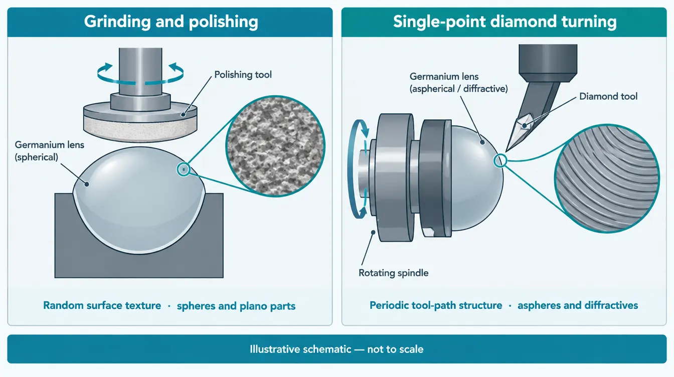
Germanium cuts in the ductile regime, so single-point diamond turning works on it directly. Conventional grinding and polishing works too. The two routes produce different parts, and a supplier that only offers one will push your design toward it.
| Route | Suits | Surface texture | Main constraint |
|---|---|---|---|
| Grinding and polishing | Spheres, plano parts, windows | Random, no periodic structure | Aspheres need dedicated tooling or sub-aperture correction |
| Single-point diamond turning | Aspheres, conics, diffractive surfaces, off-axis geometry | Periodic tool-path structure | Residual turning marks can diffract; may need post-polish |
The periodic structure left by turning matters more in some systems than others. A spectrometer or a laser path may see diffracted orders from it; a broadband thermal imager usually will not. If it matters, the drawing has to say so, because the fix — post-polishing a turned asphere — adds a process step and cannot be retrofitted after delivery. This is one of the points worth raising early when reviewing how a custom optical project moves from drawing to production, since it changes the route rather than the tolerance.
Which coating does the part actually need?
Given the reflection loss calculated above, essentially every germanium lens carries an anti-reflection coating on both surfaces. The design question is which band and which environment.
A narrow-band AR design tuned to 8–12 µm reaches higher peak transmission than a broadband design spanning 3–12 µm, because the coating stack has fewer competing targets to satisfy. If the system only images in the long wave, the broadband design is paying for spectral range it never uses. Conversely, a dual-band sensor needs the broader design and accepts lower peak values.
Exterior-facing surfaces raise a second question. Hard carbon — diamond-like carbon — is applied to outward surfaces for abrasion and rain-erosion resistance, and it is not free: the layer absorbs in the infrared, so durability is bought with transmission. That trade is normally taken on one surface only, with a conventional AR design on the protected side. Specify which surface gets which coating; do not leave it to the coating engineer to guess.
Coating requirements should also state the environmental and adhesion tests the part must survive, not just the spectral curve. Two coatings with identical transmission plots can behave differently after humidity or abrasion testing, and the difference only shows up in the field. Whoever supplies the part should be able to show how coating work sits within their broader optical fabrication and coating processes rather than treating it as an outsourced step with no traceability.
How do you verify a germanium lens you cannot see through?
This is where germanium projects separate good suppliers from optimistic ones. Germanium is opaque at visible wavelengths, so the standard 633 nm transmitted-wavefront test is unavailable. Three consequences follow.
First, surface form can still be measured in reflection at 633 nm, because a bare germanium surface reflects strongly enough for a visible interferometer to work with. A supplier who says surface figure cannot be tested at all on germanium is telling you something about their metrology, not about the material.
Second, transmitted wavefront and material homogeneity cannot be measured in the visible. They require an infrared interferometer operating inside the transmission window, typically at 10.6 µm or 3.39 µm. If your drawing calls out transmitted wavefront, ask which instrument and which wavelength will be used before the order is placed.
Third, every fringe count needs its wavelength attached. A quarter wave at 10.6 µm corresponds to a surface departure of about 2.65 µm; a quarter wave at 633 nm corresponds to about 0.16 µm. Those differ by a factor near 17. A drawing that says “λ/4” with no test wavelength is not a specification — it is a future argument. The same logic applies to roughness: total integrated scatter from a rough surface scales with (σ/λ)², so a texture that ruins a visible optic can be irrelevant at 10 µm, and paying for visible-grade roughness on a long-wave part buys nothing.
Spectral verification needs conditions too. Transmission on a germanium lens should be reported with the measurement band, the angle of incidence, and the sample temperature, because all three move the result. Acceptance criteria are per-part and per-drawing rather than universal, which is the same logic set out in a documented inspection and acceptance workflow.
Where germanium sourcing usually goes wrong
- Copying a visible-optics drawing. Scratch-dig, roughness and figure values carried over from a 633 nm part inflate cost without improving long-wave performance.
- Omitting the test wavelength. The single most common cause of an argument at incoming inspection.
- Specifying transmission with no temperature. Germanium’s absorption is temperature dependent, so a room-temperature number says little about a part running hot.
- Accepting “germanium” as the material callout. Crystal form and resistivity affect scatter and absorption and belong on the print.
- Treating coating as a line item. Band, surface assignment and durability testing are three separate decisions, not one.
- Assuming a quoted lens is a qualified lens. Ask which measurements will appear on the inspection report before the purchase order, not after.
Qualifying the supplier itself
Beyond the part, a short set of questions separates shops that handle germanium routinely from shops that will learn on your order: which fabrication routes are in-house versus subcontracted; whether infrared interferometry and infrared spectral measurement are available on site; whether the substrate is purchased as single-crystal or polycrystalline material and whether resistivity is specified on incoming material; what the coating chamber can hold in terms of part diameter and geometry; and what documentation accompanies delivery. Material traceability deserves a direct question too, since germanium substrate supply is constrained and documentation requirements vary by destination.
GIAI reviews germanium and other infrared projects against the drawing, sample, optical requirements, substrate, geometry, coating conditions and inspection criteria before defining the manufacturing route — the same review applied across the infrared optics component family and to spherical and aspheric lens fabrication. Quality-system documents, including scope and validity for any certificate, should be confirmed from the controlled certification records rather than assumed from a logo, and a management-system certificate is not a product-level performance certificate.
Frequently asked questions
What is a germanium lens used for?
Germanium lenses are used in thermal imaging, infrared sensing and infrared spectroscopy, mainly across the mid-wave and long-wave infrared. The material’s high refractive index lets designers reach a given aperture with shallower surface curvature and fewer elements, which keeps thermal camera assemblies compact. Germanium lenses appear in handheld thermal imagers, fixed thermal cameras, pyrometry and remote sensing instruments.
Why are germanium lenses so expensive?
Three factors stack up. Germanium substrate is a constrained raw material with limited primary supply. Fabrication requires either diamond turning or infrared-capable polishing rather than ordinary glass shop practice. Verification requires infrared metrology instruments that many optical shops do not own. Coating adds further cost because nearly every germanium surface needs an anti-reflection design to be usable at all.
Does germanium transmit visible light?
No. Germanium’s band gap near 0.67 eV places its absorption edge close to 1.8 µm, so it blocks visible and most near-infrared light and appears as an opaque, metallic-looking grey surface. This makes it behave as a natural long-pass element. It also means visible-light transmitted wavefront testing is impossible, and alignment through the lens requires an infrared source.
Can germanium be diamond turned?
Yes. Germanium machines in the ductile regime, so single-point diamond turning is a standard route for germanium aspheres, conics and diffractive surfaces. Single-crystal material is preferred, because cutting behaviour varies between grains in polycrystalline substrate. Turned surfaces retain a periodic tool-path structure that can diffract in some systems, so post-polishing is added when the application is sensitive to it.
What coating is used on germanium lenses?
Anti-reflection coatings are applied to both surfaces, designed either for a single band such as 8–12 µm or broadband across 3–12 µm. Outward-facing surfaces exposed to abrasion or rain erosion may instead carry a hard carbon layer, which improves durability while absorbing some infrared energy. The coating callout should name the band, the surface and the required durability tests.
References
- International Organization for Standardization. ISO 10110 (all parts), Optics and photonics — Preparation of drawings for optical elements and systems.
- International Organization for Standardization. ISO 9211 (all parts), Optics and photonics — Optical coatings.
- International Organization for Standardization. ISO 14997, Optics and photonics — Test methods for surface imperfections of optical elements.
- U.S. Department of Defense. MIL-PRF-13830B, Optical Components for Fire Control Instruments; General Specification Governing the Manufacture, Assembly, Inspection and Testing of.
- E. D. Palik (ed.), Handbook of Optical Constants of Solids, Academic Press.
- M. Bass et al. (eds.), Handbook of Optics, Third Edition, Volume IV: Optical Properties of Materials, Nonlinear Optics, Quantum Optics, McGraw-Hill / Optical Society of America.
To start a technical review, send the drawing, specification or sample together with the operating wavelength band, substrate grade and resistivity requirement, dimensions and geometry, coating requirement per surface, angle of incidence, operating temperature, inspection criteria including the test wavelength for any figure or wavefront callout, and the expected quantity.