
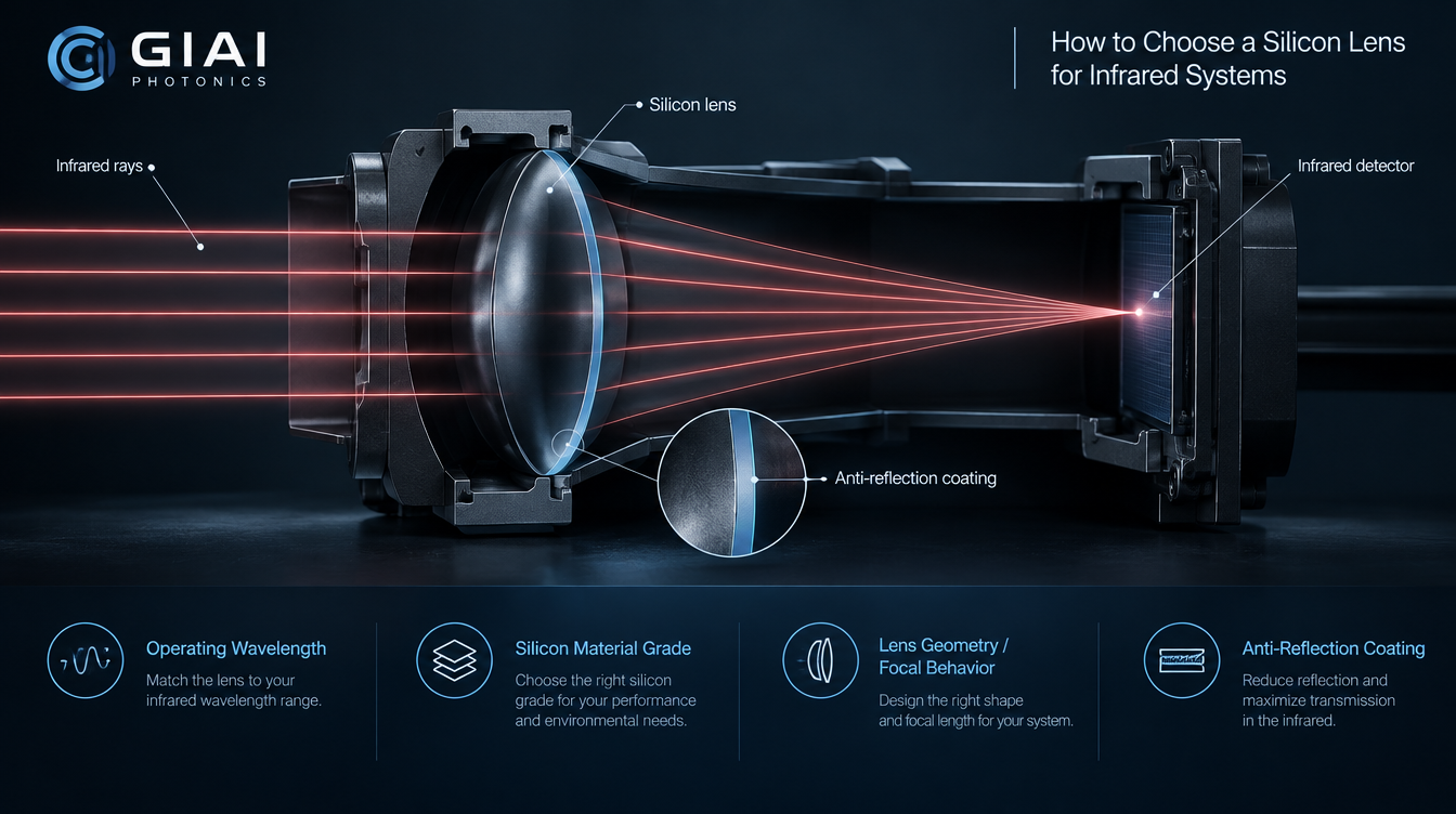
Choosing a silicon lens starts with the operating wavelength, not the lens diameter or catalog shape. Confirm that silicon is suitable for the complete spectral band, then define the optical prescription, aperture, material grade, AR coating, temperature range, mechanical interface, and acceptance criteria. For demanding infrared systems, simply specifying “silicon lens” is not enough.
Silicon is one of the infrared materials currently included in GIAI Photonics’ manufacturing scope, together with infrared lenses and related IR optical components. GIAI’s project documentation also treats material selection as a function of wavelength, geometry, coating, and operating requirements rather than material name alone.
1. Start with the wavelength range
The first question is not:
What diameter silicon lens do I need?
It is:
What wavelengths must the finished optical system transmit?
Silicon is opaque in the visible region but becomes useful as an infrared optical material beyond its absorption edge. Published optical-material data show a broad intrinsic transmission region beginning at approximately 1.2 μm, although the practically useful range depends strongly on material grade, thickness, impurity content, doping, and the requirements of the finished system.
For optical engineering, it is usually more useful to think in terms of the actual operating band rather than quoting one universal silicon transmission range.
| System requirement | Silicon lens consideration |
|---|---|
| Near-IR above the silicon absorption edge | Silicon may be suitable, but confirm detector band and material transmission |
| 3–5 μm MWIR | One of the most important practical regions for silicon optics |
| Near 8 μm and beyond | Material grade and absorption become increasingly important |
| Conventional 8–14 μm LWIR | Do not assume standard silicon is interchangeable with germanium or another LWIR material |
| Broadband IR | Review the complete transmission curve, not one nominal wavelength |
This distinction matters because bulk-material references can show silicon transmission extending to relatively long wavelengths, while real optical designs may be constrained by absorption bands, material grade, thickness, coating, temperature, and imaging requirements. Crystran, for example, lists a broad material transmission range but also notes that Czochralski-grown silicon can show an oxygen-related absorption feature near 9 μm.
GIAI’s existing comparison of germanium and silicon makes the same engineering distinction: silicon is particularly relevant to NIR/MWIR applications, while long-wave operation requires more careful qualification of the specific material.
Do not specify only “IR silicon”
A better specification identifies:
- operating wavelength or wavelength band;
- minimum required finished-lens transmission, if defined;
- detector spectral response;
- source spectrum;
- temperature range;
- coating requirement;
- relevant AOI or beam cone.
That information determines whether silicon is actually appropriate before the lens geometry is finalized.
2. Specify the silicon grade when it matters
Not every piece of silicon has identical infrared behavior.
Two common material-production routes are Czochralski-grown silicon (CZ) and float-zone silicon (FZ). Their impurity characteristics differ, and that difference can matter in infrared applications.
Published silicon material data note that oxygen associated with CZ growth can produce absorption around 9 μm, while float-zone material can be selected when this absorption is problematic. Doping and electrical resistivity can also influence longer-wave infrared transmission.
For a conventional 3–5 μm application, these details may be less critical than they are near a problematic absorption region. But once the application approaches the spectral limits of the material, writing only:
Material: Silicon
may leave too much undefined.
A more complete drawing or RFQ may need to identify the required grade, resistivity, growth process, or a defined transmission requirement.
The general rule is simple:
The closer the design operates to a material absorption feature or spectral limit, the less useful a generic material name becomes.
3. Define what the silicon lens must actually do
Once silicon has been confirmed as a suitable material, define the optical function.
A silicon lens may be required to:
- focus radiation onto an infrared detector;
- collimate radiation from an IR source;
- collect radiation from a target;
- form an image;
- couple radiation between optical subsystems;
- provide optical power inside a multi-element IR objective.
The required lens cannot be selected reliably from diameter and focal length alone.
For imaging or focusing applications, relevant system inputs can include:
| Parameter | Why it matters |
|---|---|
| Effective focal length | Determines optical power and image scale |
| Working distance | Defines the object/lens geometry |
| Back focal distance | Affects detector and mechanical packaging |
| Clear aperture | Determines usable beam area |
| f-number or numerical aperture | Influences light collection, diffraction and aberration sensitivity |
| Field of view | Strongly affects imaging-lens design |
| Detector format | Determines required image circle |
| Object distance | Changes conjugate conditions |
| Lens thickness and edge geometry | Affects mechanical integration |
| Surface form | Influences aberration correction |
GIAI’s current custom-optics workflow similarly treats lens projects in terms of optical function, focal or imaging requirement, material, clear aperture, geometry, coating, mechanical envelope, and acceptance requirements rather than one catalog parameter.
4. Account for silicon’s high refractive index
Silicon has a relatively high infrared refractive index. Published measurements put it around 3.4 in commonly used infrared regions, with the exact value varying with wavelength and temperature. For example, Crystran gives approximately 3.422 at 5 μm.
This has two important consequences.
Lens geometry changes
Optical power depends on both surface curvature and refractive index. A high-index silicon element therefore does not behave like a geometrically identical fused-silica or conventional optical-glass lens.
Changing the material while preserving the same radii is not a valid material substitution.
If an existing germanium, ZnSe, chalcogenide, or glass lens is being converted to silicon, the prescription usually needs optical re-evaluation.
Surface reflection is significant
High refractive index also creates large Fresnel reflection at an uncoated air/silicon interface.
Material data show that uncoated silicon suffers substantial two-surface reflection loss, which means the AR coating should normally be considered part of the optical design rather than an optional finishing step.
This is why a request for:
“Silicon lens, AR coated”
is incomplete.
The coating specification should instead identify the actual operating band and relevant conditions.
5. Match the AR coating to the real optical system
An AR coating optimized for one wavelength band should not automatically be expected to provide the same performance over another band.
For a silicon lens, define at least:
Operating spectral band → required transmission → AOI or beam cone → polarization if relevant → environmental requirements.
For a collimated beam close to normal incidence, coating conditions may be comparatively simple.
For a fast focusing lens, however, the coating experiences a distribution of incidence angles across the converging or diverging beam. In that case, the coating should be evaluated together with the lens numerical aperture rather than only at 0° AOI.
GIAI’s current engineering process explicitly reviews substrate, coating, wavelength region, operating geometry, and inspection criteria together for custom optics.
This becomes particularly important when:
- the bandwidth is wide;
- the lens has a low f-number;
- polarization matters;
- several coated surfaces are present;
- transmission efficiency is critical.
6. Check temperature before finalizing the lens
Silicon’s refractive index changes with temperature.
Published material data give a positive thermo-optic coefficient, meaning a temperature change can alter optical power and therefore focus position.
The practical question is not whether silicon has a temperature coefficient—it does.
The useful question is:
Will the complete optical assembly remain within its required focus, wavefront, or image-quality limits across the operating temperature range?
The answer depends on more than the lens material.
Temperature can also change:
- lens spacing;
- barrel dimensions;
- detector position;
- mounting stress;
- coating behavior;
- mechanical interfaces.
For an infrared sensor operating only near room temperature, this may have limited impact.
For automotive, outdoor, airborne, industrial, or other wide-temperature systems, thermal behavior should be part of the original lens specification rather than investigated only after focus drift appears.
7. Choose spherical or aspheric geometry based on the optical requirement
Silicon can be used in different lens forms, but the material alone does not determine whether the lens should be spherical or aspheric.
A spherical silicon lens may be sufficient when aperture, field angle and imaging requirements are moderate.
An aspheric silicon lens may help control spherical aberration or reduce element count in some systems, particularly where aperture or packaging is demanding.
However, an asphere is not automatically superior.
The decision depends on:
- aberration budget;
- field of view;
- aperture;
- focal length;
- detector size;
- working distance;
- number of optical elements;
- manufacturing and inspection requirements.
GIAI’s current public manufacturing scope includes spherical, aspheric, cylindrical, infrared and other lens forms for custom projects. The project reference likewise identifies infrared lenses as part of GIAI’s lens direction.
8. Do not overlook clear aperture, centration and mounting
A lens can have the correct outside diameter but still provide insufficient usable optical area.
The clear aperture defines the region over which the required optical performance applies. The outer mechanical diameter may include space for edge features, bevels, coating transitions or mounting. GIAI’s current technical guidance distinguishes these two dimensions explicitly.
For a silicon lens drawing, consider whether the application needs definitions for:
- outside diameter;
- clear aperture;
- center thickness;
- edge thickness;
- surface radii or aspheric coefficients;
- centration or decenter;
- bevel or edge condition;
- coating area;
- mounting datum;
- mechanical interface.
Silicon is mechanically hard compared with some IR materials, but it remains a brittle crystalline optic. Hardness should therefore not be interpreted as permission to use uncontrolled clamping force or ignore edge protection.
Mounting conditions can influence optical performance just as they do with other precision lenses.
9. Specify only the optical tolerances the system actually needs
A common sourcing mistake is to copy a demanding optical drawing from another component and apply every tolerance to the silicon lens.
That can increase manufacturing difficulty without improving system performance.
Instead, derive the specifications from the optical error budget.
Depending on the application, relevant acceptance characteristics may include:
- dimensional tolerances;
- focal length;
- centration;
- surface figure;
- surface imperfections;
- clear aperture;
- coating performance;
- transmitted wavefront;
- optical transmission;
- mechanical interface dimensions.
Not every silicon lens requires all of these to the same level.
GIAI’s manufacturing documentation therefore recommends defining inspection around the actual drawing and agreed project requirements rather than assuming one universal tolerance set for every optic.
10. Verify the finished lens, not just the raw silicon
A material datasheet tells you about the substrate.
Your optical system uses a finished lens.
Those are not the same thing.
Final performance can depend on:
material grade + thickness + surface geometry + polishing + coating + mounting + temperature.
For that reason, acceptance criteria should correspond to the characteristic that matters to the system.
For example, a project may require verification of:
- dimensions and geometry;
- focal characteristics;
- surface condition;
- coating performance over the defined wavelength band;
- clear aperture;
- project-defined wavefront or imaging characteristics.
For coated infrared components, transmission should be evaluated under measurement conditions that correspond to the intended specification.
GIAI’s documented quality approach is based on requirement review, process inspection, optical verification where required, final inspection, and project-defined acceptance criteria.
11. Common mistakes when choosing a silicon lens
The most frequent problems are often specification problems rather than material problems.
Choosing silicon from a generic transmission-range chart.
A chart does not account for material grade, thickness, impurities, temperature or the finished coating.
Writing only “AR coating.”
The coating supplier still needs the wavelength band, AOI or beam geometry, and required performance.
Changing an existing IR lens material without redesigning the prescription.
Different refractive indices change optical power and aberrations.
Ignoring the detector.
A lens should be evaluated against the detector’s active area and spectral response, not just the source wavelength.
Ignoring temperature.
For systems with a wide operating temperature range, both thermo-optic and mechanical effects can move focus.
Specifying every tolerance as tightly as possible.
A useful specification controls the parameters that affect system performance rather than maximizing manufacturing difficulty.
A Practical Silicon Lens Selection Workflow
For most projects, the selection process can be reduced to eight engineering decisions:
- Define the complete operating wavelength band.
- Confirm that the required silicon grade is suitable across that band.
- Define the optical function: imaging, focusing, collimation or collection.
- Specify focal length, aperture, working distance, field and detector constraints.
- Determine spherical, aspheric or multi-element requirements from the optical design.
- Design the AR coating for the real wavelength and angular conditions.
- Check temperature, mounting and environmental conditions.
- Define measurable acceptance criteria before manufacturing begins.
If these eight items are known, the phrase “silicon lens” becomes an engineering specification instead of only a material description.
Working with GIAI Photonics on a Custom Silicon Lens
GIAI Photonics’ current manufacturing scope includes optical lenses, infrared optics and silicon among its published optical materials. Custom projects can begin from drawings, specifications or existing samples, with manufacturing feasibility evaluated against material, geometry, coating and inspection requirements.
For a silicon lens inquiry, useful inputs include the operating wavelength, optical function, drawing or lens prescription, focal length, clear aperture, silicon grade if defined, coating requirement, AOI or numerical aperture, operating temperature, mechanical envelope, inspection criteria and expected quantity.
That information allows the lens to be evaluated as part of the actual infrared optical system rather than as an isolated piece of silicon.
FAQ
Is silicon a good material for infrared lenses?
Yes, when its transmission region matches the application. Silicon is particularly relevant to near-infrared and MWIR systems, including many 3–5 μm applications. It should not be selected simply because the application is described as “infrared,” because IR covers a very broad wavelength range and silicon behavior becomes material-grade dependent at longer wavelengths.
Can a silicon lens be used at 8–14 μm?
It should not be assumed from a generic silicon datasheet. Some high-purity or specially specified silicon can show longer-wave transmission, but absorption depends on growth method, oxygen content, resistivity, doping and thickness. Conventional LWIR systems therefore require grade-specific transmission data and complete optical validation before silicon is selected.
Does a silicon lens need an AR coating?
In most transmission applications, an appropriate AR coating is highly important because silicon’s high refractive index produces substantial Fresnel reflection at uncoated surfaces. The coating should be specified for the actual operating band, incidence-angle range and other relevant system conditions rather than simply as “AR.”
What is the difference between CZ and FZ silicon for infrared optics?
CZ and float-zone silicon differ in their impurity characteristics. Published optical-material data note that oxygen associated with CZ material can create absorption around 9 μm, while FZ material can avoid this particular issue. Whether that matters depends on the operating wavelength and the required transmission.
What information should I send for a custom silicon lens?
Provide the operating wavelength, optical function, focal or imaging requirement, material or silicon grade, dimensions, clear aperture, coating requirement, beam geometry or AOI, temperature and environmental conditions, relevant optical tolerances, drawing or sample where available, inspection requirements and quantity. This matches GIAI’s current requirement-review approach for custom lenses and other optical components.