
Technical Resources
V-Coat vs Broadband AR Coating: Specs and Trade-Offs
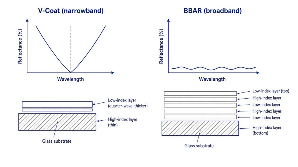
Use a V-coat when the optic sees one laser line and you need the last fraction of a percent of transmission. Use a broadband anti-reflection (BBAR) coating when the optic has to work across a spectral band, or when a second wavelength such as an alignment beam or a fluorescence return shares the same aperture. The V-coat vs broadband anti-reflection coating decision looks simple stated that way, but the consequences show up later in the build: usable bandwidth, angle tolerance, ghost reflections, layer count, laser damage threshold, and cost.
The problem both coatings solve
Light reflects at every index discontinuity. At normal incidence the Fresnel reflectance of a single air-to-glass interface is:
R = ((n_s − n_0) / (n_s + n_0))²
For N-BK7 (n ≈ 1.517 at 587.6 nm) in air, that gives R ≈ 4.2% per surface. A plano-convex lens loses about 8% of the incident power to reflection alone, and a ten-surface objective loses roughly a third of it. Worse than the loss is where that light goes: it becomes ghost images, stray light on the detector, and back-reflection into a laser cavity or fiber.
A thin-film anti-reflection coating cancels that reflection by interference. A single quarter-wave layer of index n₁ produces zero reflectance at the design wavelength when:
n₁ = √(n₀ · n_s), with optical thickness n₁d = λ₀/4
For N-BK7 in air the ideal index is 1.232. No durable coating material has that index. Magnesium fluoride (MgF₂, n ≈ 1.38) is the closest practical option, and it leaves a residual reflectance of about 1.3% at the design wavelength. That gap between the ideal index and the available materials is why every serious AR coating uses more than one layer.
What a V-coat actually is
A V-coat is a narrowband AR coating, typically two to four layers, that drives reflectance to a deep minimum at one design wavelength (DWL). The name comes from the shape of the reflectance-versus-wavelength curve, which forms a narrow V with its point at the DWL.
The most common two-layer form places a thin high-index layer (tantalum pentoxide Ta₂O₅ at n ≈ 2.1, niobium pentoxide Nb₂O₅ at n ≈ 2.3, or titanium dioxide TiO₂) directly on the substrate, then a quarter-wave of silicon dioxide (SiO₂) or MgF₂ on top. The high-index layer is not a quarter wave. Its job is to make the substrate look optically like a higher-index material, so that the low-index top layer becomes the correct index match. With that trick, the residual reflectance at the DWL can be pushed well below the single-layer limit.
Typical specified performance is R_abs < 0.25% at the DWL per surface. Optimized designs reach 0.1%, and ion beam sputtered (IBS) coatings are quoted by some suppliers below 0.05%. The catch is that the curve is roughly parabolic near its minimum, so reflectance climbs quickly on either side. Exactly how quickly is design dependent and should be read off the supplier’s measured curve, not assumed.
What a broadband AR coating actually is
A BBAR coating uses more layers, usually four to eight for a single-octave band and considerably more for multi-octave designs, to hold reflectance low across a defined wavelength range instead of at a point. Rather than one deep null, the design produces a shallow ripple with several shallow minima inside the band.
Common commercial bands and their typical per-surface specifications:
| Band | Typical specification | Notes |
|---|---|---|
| 350–700 nm (visible) | R_avg < 0.5% per surface | Standard visible BBAR |
| 650–1050 nm (NIR) | R_avg < 0.5% per surface | Covers most diode and Ti:sapphire work |
| 1050–1700 nm (SWIR) | R_avg < 0.5% per surface | Telecom and SWIR imaging |
| 400–1100 nm (wide) | R_avg < 1.0–1.5%, R_abs < 3% | Wider band costs performance |
| 3–5 µm / 8–12 µm | R_avg < 1.5% typical | Fluoride and ZnS/ZnSe/Ge layer systems |
Notice the last two rows. Bandwidth and residual reflectance are in direct competition, so stretching the band loosens the specification.
Also notice that BBAR specifications are usually written as R_avg, the reflectance averaged over the band, sometimes with a separate R_abs ceiling. A coating can meet R_avg < 0.5% while exceeding 1% at a band edge. If your laser sits at a band edge, R_avg tells you almost nothing useful.
V-coat vs broadband anti-reflection coating: parameter comparison
| Parameter | V-coat | BBAR coating |
|---|---|---|
| Design target | One wavelength (DWL) | A wavelength band |
| Typical layer count | 2–4 | 4–8, more for wide bands |
| Typical residual R (per surface) | < 0.25% at DWL, 0.1% achievable | R_avg < 0.5% over band |
| Spec form on datasheet | R_abs at DWL | R_avg over band, sometimes R_abs ceiling |
| Useful bandwidth | Narrow, design dependent | The full specified band |
| AOI tolerance | Narrow, shifts off the laser line quickly | Usually specified 0–30°; edges degrade first |
| Polarization sensitivity at AOI | Grows quickly with angle | Grows with angle, s and p diverge |
| Laser damage threshold | Generally higher, fewer and thicker layers | Lower on average, more interfaces |
| Coating run cost and yield | Lower layer count, but tight DWL centering | More layers, longer runs, more monitoring risk |
| Best fit | Single-line lasers, intracavity optics, fiber laser optics | Imaging, broadband illumination, multi-wavelength systems |
Two entries deserve comment. Laser damage threshold (LIDT) is not automatically higher for V-coats. Fewer interfaces help, but deposition process, material choice, and substrate polish quality dominate. Ion-assisted deposition (IAD) and IBS produce dense, environmentally stable films, while evaporated fluoride designs are often preferred for high-energy nanosecond pulses. Ask for LIDT tested per ISO 21254 at your pulse duration, repetition rate, and wavelength.
Cost is also not simply a layer count. A V-coat design has to land its minimum on your laser line, and chamber non-uniformity of a percent or two shifts the whole stack, so V-coat yield depends on tooling and witness monitoring.
Angle of incidence: where both coatings quietly fail
Every interference coating shifts to shorter wavelengths as the angle of incidence (AOI) increases, because the optical path through each layer changes. The shift follows:
λ(θ) = λ₀ · √(1 − (n₀ sin θ / n_eff)²)
where n_eff is the effective index of the layer stack, typically somewhere between the low and high index materials. Using n_eff = 1.75 as an illustration for a 1064 nm design:
| AOI | Effective center wavelength | Shift |
|---|---|---|
| 0° | 1064 nm | 0 nm |
| 10° | 1059 nm | 5 nm |
| 20° | 1044 nm | 20 nm |
| 30° | 1020 nm | 44 nm |
| 45° | 973 nm | 91 nm |
The value of n_eff varies with the actual design, so treat this table as the shape of the behavior rather than a lookup. The engineering point stands: a V-coat centered at 1064 nm for normal incidence is no longer centered at 1064 nm on the marginal rays of a fast lens or on a scanner mirror at 30°.
A BBAR coating degrades more gracefully because it has band to spare, which is why suppliers commonly specify BBAR performance for AOI from 0° to 30° (roughly 0.5 numerical aperture) rather than at a single angle. Beyond about 30°, s and p polarization reflectance diverge noticeably, and the coating should be redesigned for the working angle. A coating optimized for 45° is a different design, not the same design used off-label.
For high-numerical-aperture optical lenses and fast objectives, specify the AOI range across the clear aperture, not just the chief ray angle.
Reading the rest of the datasheet
Reflectance is only part of the specification. The parameters that determine whether the part works in your system:
- Per surface or per element. A “< 0.5%” figure almost always means per surface. Two coated surfaces on a window give roughly 1% total reflective loss.
- R_avg versus R_abs. Ask for both, plus the measured curve. Average reflectance hides band-edge behavior.
- Clear aperture. Coating uniformity degrades near the edge of the tooling. Specify the diameter over which the reflectance spec applies, typically 85–90% of the physical diameter.
- Surface quality (scratch-dig). Specified per MIL-PRF-13830B, or per ISO 10110-7 in Europe. Common values are 60-40 for general use, 40-20 for imaging, 20-10 or 10-5 for laser optics. Coating does not hide substrate defects; it decorates them.
- Surface figure. Quoted as peak-to-valley in fractions of a wavelength at 632.8 nm, commonly λ/4 for general use and λ/10 for laser and interferometric work. Coating stress can change the figure on thin substrates, which matters when the diameter-to-thickness ratio exceeds roughly 10:1.
- Environmental durability. Adhesion, humidity, abrasion, temperature cycling, and salt fog, typically referenced to ISO 9211 or the older MIL-C-48497A and MIL-C-675C durability specifications. A coating that passes moderate abrasion may not pass severe abrasion.
- Substrate compatibility. The layer design is substrate specific. A V-coat design for fused silica is not the same design for sapphire, silicon, or zinc selenide.
Common specification mistakes
Specifying a V-coat for a system that has two wavelengths. This is the most expensive mistake in this category. A 1064 nm laser processing head with a 650 nm red alignment diode, both passing through the same V-coated optics, will show 3% to 4% reflectance per surface at the alignment wavelength. Across six surfaces the visible alignment beam loses a fifth of its power, and those reflections travel back down the beam path. In a fiber laser build, that returning energy can reach the isolator or the fiber facet.
Reading R_avg and assuming it applies at your line. A 400–1100 nm BBAR coating with R_avg < 1.0% may sit near 2% at 405 nm. If a 405 nm diode is your source, you specified a coating that is four to eight times worse than the number you read.
Specifying at 0° AOI and using the optic in convergent light. In an f/1.4 system, marginal rays hit the surface near 20°, well past the point where a narrowband coating has moved off its design wavelength.
Ignoring coating stress on thin windows. A multi-layer BBAR stack on one side of a 1 mm thick, 50 mm diameter window can bow it measurably. Coat both sides, or budget for figure change.
Not specifying the environmental class. A coating that meets your reflectance number in the lab may not survive cleaning, humidity, or a thermal cycle in the field.
How to choose
Ask four questions in order.
- How many wavelengths pass through this surface? More than one, including alignment, pump, and signal return, means BBAR or a dual-band design.
- What is the source linewidth and tuning range? A single-frequency laser suits a V-coat. A tunable, temperature-drifting, or multimode source needs margin.
- What is the AOI range across the clear aperture? Not the chief ray. The full cone.
- What is the power density, and is it continuous wave or pulsed? This drives material and process selection more than the reflectance spec does.
If the answers are one wavelength, narrow linewidth, near-normal incidence, and high power density, the V-coat is the right part. Anything else, and the BBAR coating is usually the safer engineering choice even though its number at the laser line looks worse. GIAI Photonics supplies both single-wavelength and broadband coatings on optical lenses, windows, and prisms, including designs on infrared substrates.
FAQs
Can I use a V-coat across a laser diode’s tuning range? It depends on the tuning range and the design. A distributed feedback diode drifting a few nanometers with temperature is usually fine. An external cavity diode tuning over tens of nanometers is not, because the V-coat reflectance climbs steeply away from the design wavelength. Ask the supplier for the measured curve and check the reflectance at both tuning extremes.
Is a V-coat always lower loss than a BBAR coating at the laser line? At the exact design wavelength and design angle, yes, usually by a factor of two to five. Away from either condition the advantage disappears quickly. In a real system with beam convergence, thermal drift, and manufacturing tolerance, a good BBAR coating often delivers more consistent throughput than a V-coat that is slightly off center.
Do I need the coating on both surfaces? Almost always. An uncoated second surface contributes roughly 4% loss and generates a ghost that interferes with the first surface reflection. The only common exception is a surface that is cemented, contacted, or immersed, where the index step is small and a different design applies.
Which coating has the higher laser damage threshold? Generally the V-coat, because it has fewer layers and fewer interfaces where absorbing defects accumulate. But deposition process, material selection, and substrate polish matter more than layer count. Request LIDT data measured per ISO 21254 at your wavelength, pulse duration, and repetition rate rather than comparing headline numbers.
Can one coating handle both 1064 nm and 532 nm? Yes, with a dual-band or multi-V design that places separate minima at each line. This costs more layers than a single V-coat and gives up performance between the lines, which is acceptable when nothing operates there. It is the standard approach for frequency-doubled Nd:YAG systems.
For a specific design wavelength, band, angle, and substrate, send the requirement to the GIAI Photonics custom optical coatings team and ask for the modeled reflectance curve before committing to a build.