
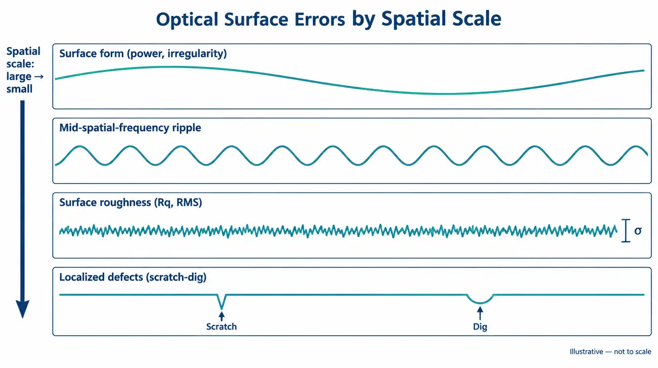
- Scratch-dig limits discrete local defects; surface roughness is the RMS height of fine texture across the whole surface.
- The MIL-PRF-13830B scratch number is a visibility grade, not a width; the dig number is diameter in 0.01 mm.
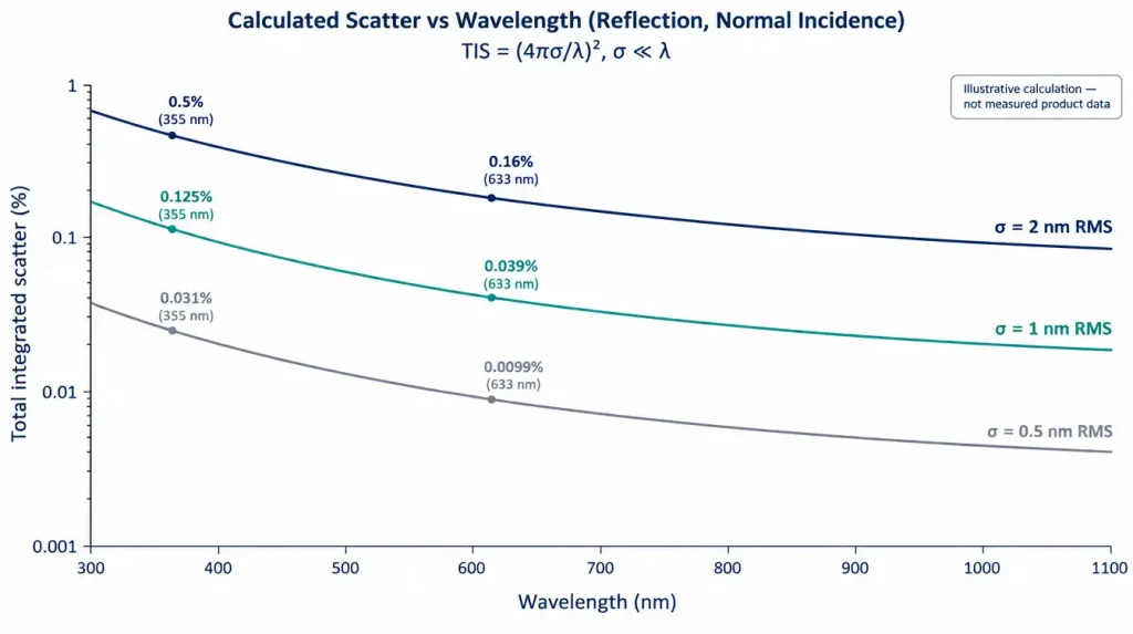
- Roughness-driven scatter scales with (σ/λ)², so the same surface scatters four times more at half the wavelength.
- A dig’s impact depends on where the surface sits: minor far from focus, visible near an image plane.
- Specify both per surface, with the governing standard, clear aperture, spatial band and inspection conditions.
Scratch-dig and surface roughness are two separate specifications for a polished optical surface. Scratch-dig limits localized defects: scratches graded by visibility and digs graded by diameter, under MIL-PRF-13830B or ISO 10110-7. Surface roughness, usually stated as RMS height (Rq), describes the fine texture of the whole surface and governs diffuse scatter. Meeting one says nothing about the other.
The two are easy to confuse because both appear on the surface quality line of a drawing, and some datasheets use the terms interchangeably. They are inspected with different instruments, they fail parts for different reasons, and they add cost at different stages of fabrication. This article explains what each number means, how each affects transmission, scatter and image quality, and how to write both on a drawing so supplier and customer inspect to the same criteria. For related tolerancing topics, see the lens and optical component engineering resources.
What does a scratch-dig specification measure?
A scratch-dig specification limits discrete, localized imperfections inside the clear aperture. The first number grades the worst allowed scratch by its apparent brightness. The second number sets the largest allowed dig diameter. A 60-40 surface allows scratches no more visible than the #60 reference scratch and digs no larger than 0.40 mm.
Under MIL-PRF-13830B, the scratch number is assigned by visual comparison against calibrated master scratches under controlled illumination. It is a visibility grade. It should not be read as a width in micrometres measured on the part. Because the comparison is visual, two inspectors can grade the same scratch differently, and so can a supplier and a customer who use different lighting.
The dig number is dimensional. It is the diameter of the largest permitted dig in units of 0.01 mm, so dig 10 means 0.10 mm and dig 40 means 0.40 mm. The specification also restricts how many maximum-size scratches and digs may be present, and how close together they are, relative to the clear aperture. These accumulation rules decide many acceptance disputes, so read them from the standard rather than assuming them.
ISO 10110-7 takes a dimensional approach. On an ISO drawing, surface imperfections carry code 5. A callout of the form 5/ N × A limits the number N of imperfections and their grade number A, which is the square root of the imperfection area in millimetres. Further indications control coating imperfections (C), long scratches (L) and edge chips (E). ISO 14997 describes the corresponding test methods. Drawings prepared to the Chinese standard GB/T 1185 use their own class designations. None of these systems converts exactly into another, so the drawing must name the standard that governs acceptance.
What does surface roughness measure on an optical surface?
Surface roughness describes the random, high-spatial-frequency height variation that the final polishing step leaves across the whole surface. Optical drawings normally state it as RMS roughness, Rq, in nanometres or ångströms (1 Å = 0.1 nm). It is a statistical property of the surface. It does not count individual defects.
Rq is the root-mean-square deviation of surface height from the mean plane within the evaluated area. Ra, the arithmetic mean of the absolute deviations, is common on mechanical drawings but less useful in optics, because scatter theory is written in terms of RMS height. For a surface with a Gaussian height distribution, Rq = √(π/2) × Ra, a ratio of 1.25. Polishing grooves, pits or other non-Gaussian texture change that ratio, and then Ra and Rq cannot be converted without the measured profile.
A roughness value means little without its spatial-frequency band. A white light interferometer with a wide field of view, the same instrument with a high-magnification objective, and an atomic force microscope each sample a different range of surface wavelengths. They can report different Rq values on the same sample. ISO 10110-8 covers the drawing indication for surface texture. A complete callout gives the RMS value together with the band it applies to, or with the instrument, objective and filtering used. Roughness should be measured on defect-free areas, because a scratch inside the measurement window dominates the RMS result.

How do scratch-dig and surface roughness differ?
The two specifications differ in what they describe, how they are inspected and which optical loss they control. Scratch-dig is a pass/fail limit on the worst local defects, inspected mainly by eye or by imaging. Roughness is an area-averaged statistic measured with an interferometric or probe instrument.
| Specification | Controls | Notation | Standards | Inspection | Output | Optical effect |
|---|---|---|---|---|---|---|
| Scratch-dig | Discrete scratches, digs, coating and edge defects | 60-40 (visibility); 5/ N × A (ISO) | MIL-PRF-13830B, ISO 10110-7, ISO 14997 | Visual comparison to masters, dark-field viewing, microscopy | Pass/fail against a grade | Local obscuration, localized scatter, possible laser damage sites |
| Surface roughness | Random fine texture over the whole surface | Rq in nm or Å RMS, with spatial band | ISO 10110-8, ASME B46.1 | White light interferometry, AFM, stylus profilometry, scatter measurement | Numeric value within a stated band | Diffuse scatter across the aperture, contrast loss |
The two also have different sources in the shop. Scratches and digs come mostly from particles caught during polishing and from handling, cleaning and packing. Roughness is set by the polishing process itself: lap material, polishing compound, process duration, and how the substrate material responds to them. A surface can therefore pass a tight scratch-dig grade and still be relatively rough, and a superpolished surface can fail inspection because of a single scratch.
How does each specification affect optical performance?
Roughness sets a scatter floor over the whole illuminated aperture, and that floor rises steeply at short wavelengths. Scratch-dig defects remove or redirect light only where they sit. Their effect therefore depends mainly on where the surface is in the optical path and how the beam fills it.
Roughness and total integrated scatter
For a smooth surface (σ much smaller than λ), total integrated scatter estimates the fraction of reflected light scattered out of the specular beam at normal incidence: TIS = (4πσ/λ)². Here σ is the RMS roughness within the spatial-frequency band that scatters into the angles of interest. Scatter grows with σ² and falls with λ², so halving the wavelength quadruples the scatter from the same surface.
| Wavelength | σ = 0.5 nm | σ = 1 nm | σ = 2 nm |
|---|---|---|---|
| 355 nm | 0.031% | 0.125% | 0.50% |
| 633 nm | 0.0099% | 0.039% | 0.16% |
| 1064 nm | 0.0035% | 0.014% | 0.056% |
| 10.6 µm | 0.000035% | 0.00014% | 0.00056% |
For a transmitting surface at normal incidence, the corresponding estimate is TIS = [2πσ(n − 1)/λ]². For fused silica at 633 nm (n = 1.457) with σ = 1 nm, this gives 0.0021% (calculated). That is a factor of 19 below the 0.039% calculated for the same roughness in reflection. For this reason, mirror substrates and other reflecting surfaces are where a tighter roughness limit is most likely to be worth its cost. A thin-film coating tends to replicate the roughness of the substrate and adds some of its own, so coating a rough substrate does not make it smooth.

Scratches and digs: position in the beam decides
A dig on a surface far from focus blocks a small fraction of the beam area and is not imaged. As a calculated example, a single 0.40 mm dig (the limit for dig 40, treated as a circular opaque spot) on a 25 mm diameter clear aperture covers 0.026% of the aperture area. The same dig on or near an image plane, a field stop or a reticle is imaged sharply. On a sensor cover glass it casts a shadow onto the sensor. At a 5 µm pixel pitch, a 0.40 mm feature spans 80 pixels.
Scratches and digs also scatter light locally. This becomes visible in dark-field illumination, in low-light imaging, and in systems with bright sources close to the field of view. In laser beam delivery optics, the edges of polishing defects and residues trapped in them can absorb energy and initiate laser-induced damage. Scratch-dig grade is not a damage threshold, though. Parts with the same grade can show different LIDT, so laser optics need a damage threshold requirement tested at the actual wavelength, pulse duration and beam conditions.
What do scratch-dig and roughness not cover?
Neither specification describes surface form, mid-spatial-frequency error or subsurface damage. Each of these needs its own callout, and a surface can pass both scratch-dig and roughness while failing on any of them.
Surface form error, meaning power and irregularity (ISO 10110-5), is measured with a full-aperture interferometer and sets transmitted or reflected wavefront error. Mid-spatial-frequency ripple, often left by sub-aperture polishing, lies between form and roughness in scale. It can produce small-angle scatter or periodic image artefacts that neither a roughness measurement nor a visual inspection may reveal. Subsurface damage from grinding can remain beneath a polished surface that looks clean and measures smooth. It can open up later during etching, coating or laser exposure.
What does tightening each specification cost?
Tighter scratch-dig grades and lower roughness are paid for in different places. Scratch-dig cost comes mainly from inspection, rework and rejected parts. Roughness cost comes from longer or additional polishing stages and depends strongly on the substrate. Over-specifying either one adds cost without a measurable gain in system performance.
- Scratch-dig. Each tighter grade raises the share of parts rejected or sent back for repolishing. It also demands cleaner handling through coating and packing, and it makes grading more sensitive to inspection conditions. For a fixed grade the permitted defect size stays the same while the aperture area grows with the square of the diameter, so a given grade has less optical impact on a larger part.
- Roughness. A lower RMS target can require an extra fine-polishing or superpolishing stage. Crystalline and polycrystalline materials respond to polishing differently from amorphous glasses, so a roughness value achieved on fused silica cannot be assumed for sapphire, silicon, germanium or ZnSe without project-level review.
- Wavelength. Because scatter scales with λ⁻², a roughness limit that matters on an ultraviolet surface can be irrelevant on a long-wave infrared window. A tight scratch-dig grade on such a window rarely improves system performance unless the surface sits near focus.
- Verification. Roughness is measured at sampled locations. The number of locations and parts measured sets both the inspection cost and the confidence in the result, so it belongs in the agreed acceptance plan.
How should scratch-dig and roughness be specified on a drawing?
Specify each surface individually, based on its position in the optical path and the working wavelength, and name the governing standard and inspection conditions for both callouts. A single line such as “60-40, 5 Å” copied onto every surface of an assembly is a common source of both unnecessary cost and disputed acceptance.
- Classify each surface: at or near an image plane or field stop, in a focused or high-fluence laser beam, in a reflective path, or in a large collimated beam far from focus.
- Name the standard for surface imperfections, MIL-PRF-13830B or ISO 10110-7, and do not mix notations on one drawing without stating which one governs.
- Define the clear aperture where the grade applies, and give a separate, looser requirement outside it if needed.
- State roughness as Rq with its spatial-frequency band or measurement setup, and state whether it applies to the bare substrate or the coated surface.
- Agree inspection conditions and acceptance criteria before production: illumination, viewing in reflection or transmission, magnification, reference masters and the roughness sampling plan.
- Add surface form, subsurface damage and LIDT requirements as separate callouts where the application depends on them.
Common mistakes
- Reading the scratch number as a scratch width, which leads to rejecting or accepting parts on a measurement the standard does not use.
- Assuming a tight scratch-dig grade guarantees low roughness, or the reverse.
- Quoting an RMS value with no spatial band or instrument, so that supplier and customer measurements cannot be compared.
- Using “surface quality” and “surface finish” on a drawing without defining which specification each term refers to.
- Applying a sensor-window grade to large protective optical windows far from focus, where it adds cost without affecting the image.
- Expecting a coating to hide substrate scratches or roughness. Coatings follow the substrate surface and can make defects more visible in reflection.
Frequently asked questions
What does 60-40 scratch-dig mean?
A 60-40 scratch-dig specification under MIL-PRF-13830B allows scratches no brighter than the #60 calibrated reference scratch and digs no larger than 0.40 mm in diameter within the clear aperture. The 60 is a visibility grade assigned by visual comparison, not a width measurement. The 40 is dimensional, expressed in units of 0.01 mm. The standard also limits how many maximum-size defects may be present.
Is scratch-dig the same as surface roughness?
Scratch-dig and surface roughness are different specifications. Scratch-dig limits discrete local defects such as scratches and digs and is inspected mainly by visual comparison. Surface roughness is the RMS height of the fine texture across the whole surface, measured with instruments such as white light interferometers or atomic force microscopes. A surface can meet a tight scratch-dig grade and still be rough, or be very smooth and carry a scratch.
What is the difference between Ra and RMS surface roughness?
Ra is the arithmetic mean of the absolute height deviations from the mean surface, while RMS roughness (Rq) is the square root of the mean squared deviation. Rq weights larger deviations more heavily and is the quantity used in optical scatter calculations. For a Gaussian height distribution, Rq equals √(π/2) times Ra, a ratio of 1.25. For other surface profiles the ratio differs.
How is surface roughness measured on optical surfaces?
Surface roughness on optical surfaces is measured with non-contact white light interferometers, atomic force microscopes and contact stylus profilometers, or indirectly by scatter measurement. Each method covers a different range of spatial frequencies, so the same surface can return different RMS values. A roughness specification should therefore name the spatial-frequency band or instrument settings and be measured on a defect-free area.
What scratch-dig is required for laser optics?
No single scratch-dig grade is correct for all laser optics. Tighter grades are justified where the beam is focused on or near the surface, where the wavelength is short, or where fluence is high, because defects scatter light and can initiate laser damage. Scratch-dig is not a damage threshold, so laser optics also need a laser-induced damage threshold requirement tested at the actual wavelength and pulse conditions.
References
- U.S. Department of Defense, MIL-PRF-13830B, Performance Specification: Optical Components for Fire Control Instruments; General Specification Governing the Manufacture, Assembly, and Inspection of.
- ISO 10110-7, Optics and photonics — Preparation of drawings for optical elements and systems — Part 7: Surface imperfections.
- ISO 10110-8, Optics and photonics — Preparation of drawings for optical elements and systems — Part 8: Surface texture.
- ISO 14997, Optics and photonics — Test methods for surface imperfections of optical elements.
- J. M. Bennett and L. Mattsson, Introduction to Surface Roughness and Scattering, Optical Society of America.
- D. M. Aikens, “Meaningful surface roughness and quality tolerances,” Proceedings of SPIE, International Optical Design Conference.
To have scratch-dig and roughness callouts reviewed against manufacturing feasibility, send GIAI the drawing, optical specification or sample through the custom optics review process or the project contact page, together with the wavelength range, substrate, dimensions, coating requirements, AOI, surface callouts with their governing standards, inspection criteria and expected quantity.