
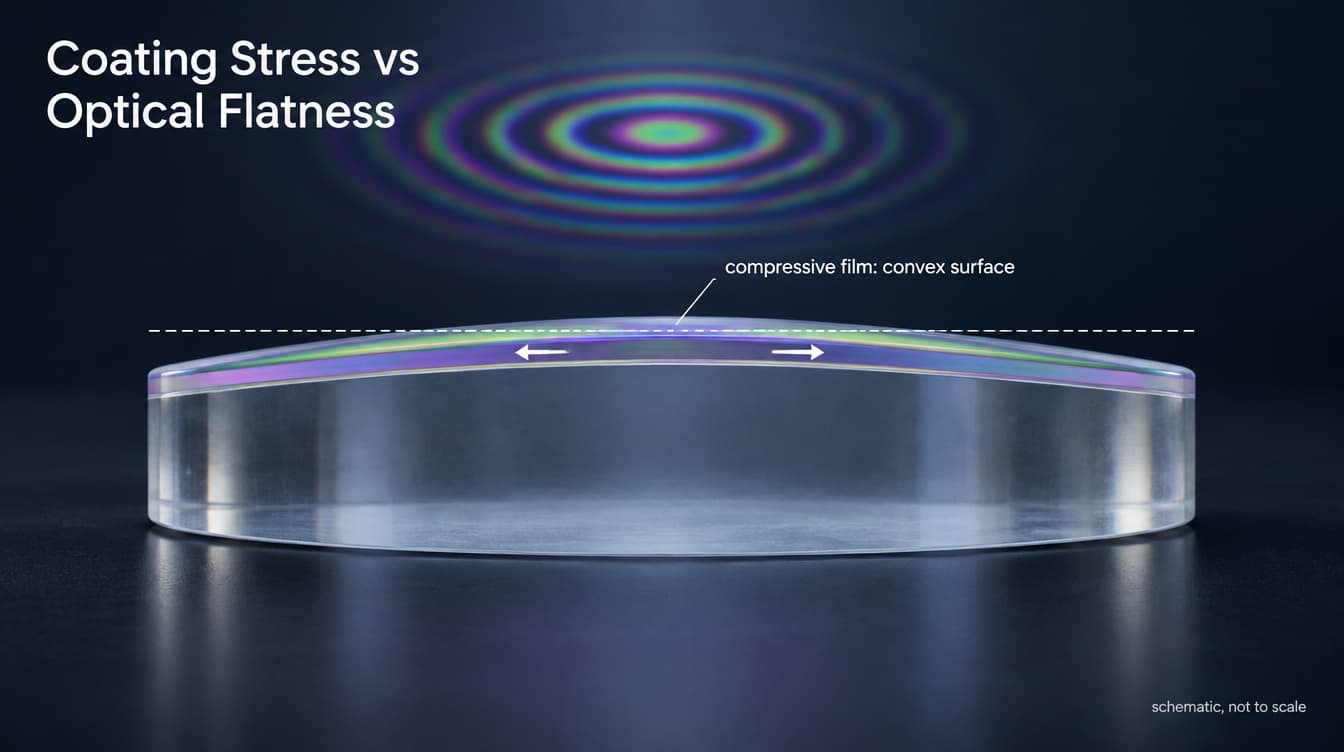
A substrate can leave polishing at λ/10 and come out of the coating chamber measuring a full wave of error. The polishing did not change. The coating did it.
Coating stress affects optical flatness by bending the substrate. A thin film that is under residual stress pulls or pushes on the surface it is bonded to, and the substrate curves until the forces balance. On a round, uniform flat this shows up mainly as power: a shallow spherical error added to the surface. The size of that error depends on the film stress, the total film thickness, and above all the substrate’s diameter-to-thickness ratio.
Why a coating bends the substrate
An optical coating is not a relaxed layer. After deposition and cool-down, the film is left in one of two states:
- Compressive stress. The film would be larger if it were free. Held by the substrate, it pushes outward and the coated surface becomes convex.
- Tensile stress. The film would be smaller if it were free. It pulls inward and the coated surface becomes concave.
The film is typically a few micrometres thick and the substrate a few millimetres. The film still wins some of the argument, because its stress can reach hundreds of megapascals and it acts at the outer surface, where it has the most leverage on bending.
The Stoney relation: what sets the size of the error
For a thin film on a much thicker, isotropic, freely supported plate, the Stoney equation links film stress to the curvature it produces:
\sigma_f = \frac{E_s\, t_s^{2}}{6\,(1-\nu_s)\, t_f\, R}Here σf is the mean film stress, tf the film thickness, ts the substrate thickness, Es and νs the substrate’s Young’s modulus and Poisson’s ratio, and R the change in radius of curvature. Combining it with the sag of a shallow sphere over diameter D gives the form an optical engineer needs:
\delta = \frac{D^{2}}{8R} = \frac{3\,(1-\nu_s)\,\sigma_f\, t_f}{4\,E_s}\left(\frac{D}{t_s}\right)^{2}Three things follow directly:
- Stress and film thickness act as a product. A thick stack at moderate stress bends the part as much as a thin stack at high stress. Long-wave and multi-cavity designs are at risk for this reason alone.
- Substrate thickness enters as a square. Doubling the thickness cuts the bending to a quarter.
- Aspect ratio is the lever. The error scales with (D/ts)², so a thin, wide part is far more sensitive than a small thick one.
The relation assumes uniform stress, a film much thinner than the substrate, and a deflection that is small compared with the substrate thickness. Outside those limits it is an estimate, not a prediction.
A worked example
The figures below are a calculation, not measured product data. They assume a 25.4 mm fused silica substrate (Es = 71.7 GPa, νs = 0.17), a 5 µm dielectric stack, and a mean compressive stress of 300 MPa. Sag is taken across the full diameter and expressed in waves at 632.8 nm.
| Substrate thickness | Diameter-to-thickness ratio | Calculated sag | Sag in waves at 632.8 nm |
|---|---|---|---|
| 1.0 mm | 25:1 | 8.4 µm | 13 |
| 2.0 mm | 13:1 | 2.1 µm | 3.3 |
| 3.0 mm | 8.5:1 | 0.93 µm | 1.5 |
| 5.0 mm | 5:1 | 0.34 µm | 0.53 |
| 6.35 mm | 4:1 | 0.21 µm | 0.33 |
The same coating that turns a 1 mm filter substrate into a visibly curved part still leaves the quarter-inch-thick mirror at about a third of a wave. Tight flatness after coating therefore needs deliberate stress control even on thick parts, and it becomes expensive or unrealistic on a thin filter with a thick stack.
Where coating stress comes from
The stress in a finished coating is the sum of three contributions, and they do not always have the same sign.
Intrinsic stress is built in during film growth. Energetic processes pack atoms more tightly than they would settle on their own, which produces dense, compressive films. Low-energy evaporation tends to produce a more porous, columnar structure with lower or tensile stress.
Thermal stress appears when the part cools from deposition temperature to room temperature. Film and substrate contract by different amounts, so the mismatch in thermal expansion is locked in as stress. The same mechanism makes flatness drift with operating temperature.
Environmental stress applies mainly to porous films. They absorb water from the air, which shifts stress toward compressive; in dry nitrogen or vacuum the water leaves and the stress moves toward tensile. A part measured flat in a humid lab can change shape in a purged or evacuated instrument. Dense films are much less affected.
How the deposition process changes the outcome
The tendencies below are general ones reported in the thin-film literature. Actual stress depends on materials, layer design, ion energy, rate, temperature and chamber conditions, so it has to be established for a specific process rather than assumed.
| Process | Film structure | Typical stress tendency | What it means for flatness |
|---|---|---|---|
| Electron-beam evaporation, no ion assist | Porous, columnar | Low to moderate; can be tensile and humidity-dependent | Small bending, but the shape can shift between ambient and dry or vacuum conditions |
| Ion-assisted deposition (IAD) | Dense | Usually compressive; level depends on ion energy | Stable in changing humidity, with more bending than unassisted evaporation |
| Ion beam sputtering (IBS) | Very dense, amorphous | High compressive, often hundreds of MPa | Best spectral stability and low loss, with the largest bending per micrometre of film |
| Magnetron sputtering | Dense | Compressive, process-dependent | Similar trade-off to IBS; compensation is usually needed on thin parts |
Published measurements give a sense of scale. One study of dual ion beam sputtered Ta2O5 on fused silica reported about 160 MPa compressive as deposited. Another reported 490 MPa for ion-beam-deposited SiO2 before process changes brought it down to 48 MPa.
The trade-off is real. The dense, stable films that hold a narrow passband or a steep edge in place are the same films that bend the substrate most. Choosing a process for spectral performance means accepting, and then managing, its stress.
Power, irregularity and what the system sees
Uniform stress on a round, uniform substrate produces a nearly spherical change, so the error is mostly power. Irregularity appears when the symmetry is broken: non-uniform film thickness across the aperture, rectangular or non-circular parts, wedged substrates, crystalline materials with direction-dependent stiffness, or a mount that constrains the part.
How much the error matters depends on how the component is used.
- Mirrors. The reflected wavefront error is about twice the surface error near normal incidence. A flat with added power behaves like a very weak curved mirror. Used as a 45° fold, that power appears as astigmatism, which refocusing cannot remove.
- Filters and windows in transmission. Bending turns a plane-parallel plate into a weak meniscus of nearly constant thickness. To first order this adds little transmitted wavefront error, so a filter can look poor in a reflection flatness test and still transmit a clean wavefront.
- Dichroics and beamsplitters. These work in both reflection and transmission. The reflected path carries the full bending error, and it is usually the path that sets the specification.
How to reduce stress-induced flatness error
No single method removes the effect. Each one trades against cost, spectral performance or lead time.
| Method | How it works | What it costs |
|---|---|---|
| Thicker substrate | Bending falls with the square of thickness | Weight, space and material; not available when thickness is fixed by the design |
| Backside compensating coating | A second film with a matching stress-thickness product bends the part back | An extra coating run; the back coating must also suit the optical path, for example an AR coating on a filter |
| Post-deposition annealing | Heat relaxes compressive stress; in one Ta2O5 study it fell roughly linearly with temperature and crossed zero near 591 K | Shifts the spectrum, so the design must allow for it; limited by substrate, metal layers and cemented parts |
| Process tuning | Ion energy, rate and gas conditions change intrinsic stress | Possible changes in density, refractive index and environmental stability |
| Thinner or simpler stack | Fewer layers lower the stress-thickness product | Less blocking, lower edge steepness or lower reflectance |
| Pre-figured substrate | The substrate is polished with opposite power so the coating pulls it flat | Needs repeatable stress from run to run; adds polishing and metrology effort |
A common mistake is to treat the backside coating as a matter of matching thickness. What must balance is stress multiplied by thickness on each face. Two coatings of equal thickness but different materials or processes will not cancel.
How to specify and verify flatness after coating
Most disputes over coated flats come from an incomplete specification, not from a failed process. Four points remove most of the ambiguity.
- State when the flatness applies. A drawing that says λ/10 without saying “after coating” is normally read as a polishing requirement on the bare substrate.
- Separate power from irregularity. If the system can refocus, allow more power and hold irregularity tight. Surface form notation in ISO 10110-5 supports this split. A single peak-to-valley number forces the supplier to control power that the system may not care about.
- Choose the right metric for the function. Call out reflected flatness for mirrors and dichroics. For filters and windows used in transmission, transmitted wavefront error is usually the number that matches system performance.
- Define the measurement conditions. State the test wavelength, the aperture over which the value applies, how the part is supported, and the environment if the part will run dry, in vacuum or at temperature.
Verification is a before-and-after comparison. The surface is measured on an interferometer before coating and again afterwards, over the same aperture and in the same unstressed support, and the difference is the coating’s contribution. Two practical cautions apply. A coating designed for another wavelength may reflect very little or almost everything at the interferometer wavelength, which affects fringe contrast and may require measuring the other face or a different test wavelength. And porous coatings should be measured after they have stabilised in the environment they will be used in.
What to send with an RFQ
For a coated part with a flatness or wavefront requirement, the following inputs let a supplier estimate the stress effect before quoting:
- Substrate material, diameter or dimensions, and thickness, with any freedom to change thickness
- Coating type, wavelength range, angle of incidence and polarization
- Flatness or wavefront requirement, stated as after coating, with power and irregularity separated where possible
- Clear aperture over which the requirement applies
- Whether the back surface can carry a compensating or AR coating
- Operating environment: ambient, purged, vacuum, and temperature range
- Inspection method, test wavelength and report format
GIAI reviews custom optical projects against the drawing, sample, optical requirements, substrate, geometry, coating conditions and inspection criteria before defining the manufacturing route. For coated flats, sending the flatness requirement together with the spectral specification allows substrate thickness, coating design and compensation to be considered as one problem. Project details can be submitted through the contact page.
FAQ
Does coating stress always make an optic worse?
It always changes the shape, but the change is not always a problem. On a thick substrate the added power may be well inside tolerance. In transmission, a uniformly bent plate adds little wavefront error to first order. The effect becomes critical on thin, large-aperture parts used in reflection, and on thick multilayer stacks.
Is the bending convex or concave?
Compressive film stress makes the coated surface convex. Tensile stress makes it concave. Dense ion-assisted and sputtered oxide coatings are usually compressive. Evaporated coatings made without ion assist can be tensile, and their stress can change sign with humidity.
Can a coated optic be re-polished to restore flatness?
Not on the coated face, because polishing would remove the coating. The practical routes are to compensate on the back surface, anneal where the design and materials allow, or plan ahead with a thicker or pre-figured substrate. This is why the flatness requirement needs to be known before coating, not after.
Why does flatness change when the optic goes into vacuum?
Porous coatings hold water in their microstructure. In vacuum or dry gas the water leaves, the film stress shifts toward tensile, and the substrate curvature changes with it. The spectral position usually shifts as well. Dense coatings absorb far less water and show much smaller changes.
How thick should the substrate be to hold flatness after coating?
There is no single ratio, because the answer depends on the stress-thickness product of the coating and the flatness required. Thickness has a squared effect, so it is the strongest design lever. A Stoney estimate with the expected stress and stack thickness is the right starting point, followed by confirmation on a coated test piece.