
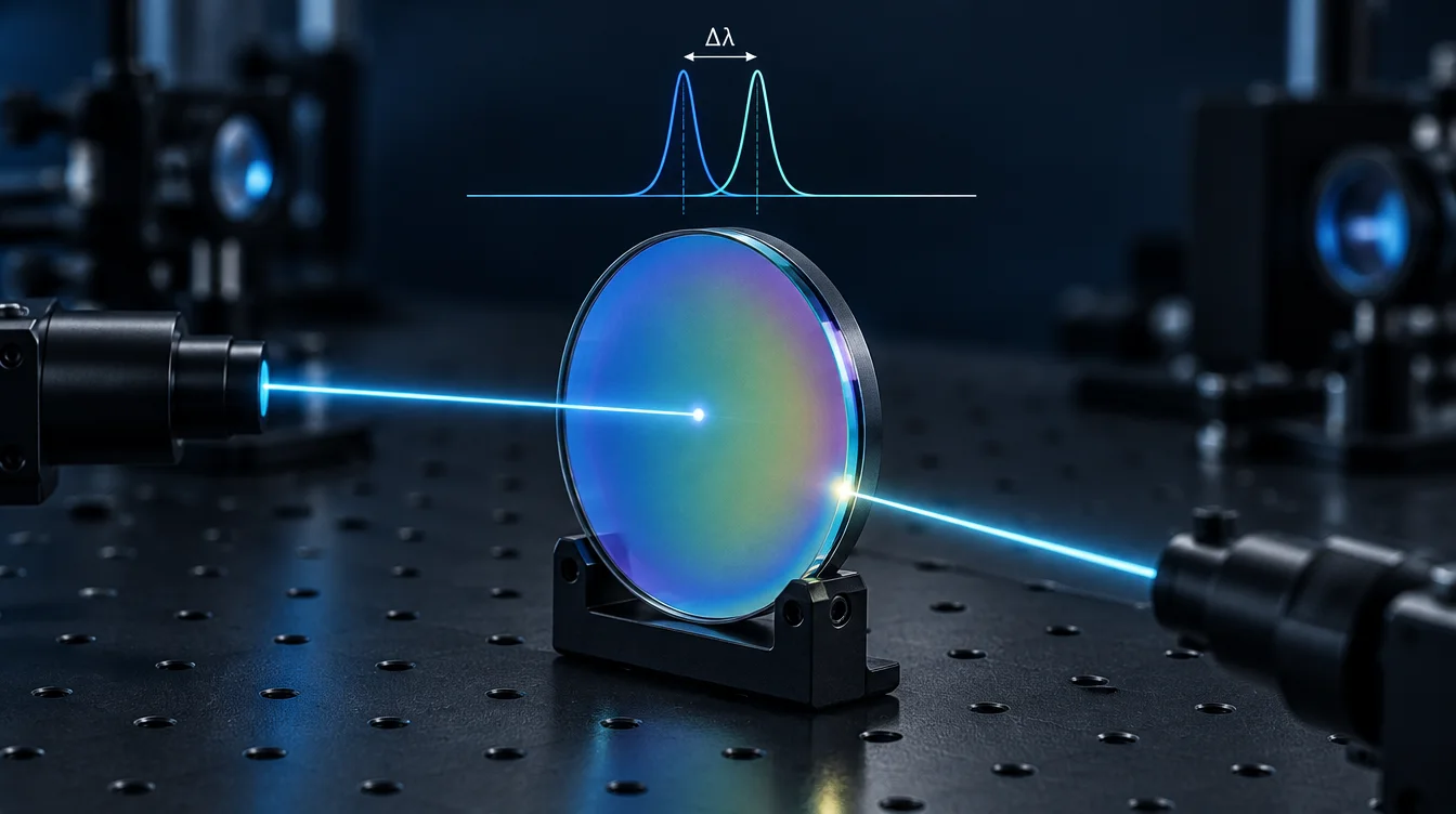
A coating that meets its spectrum at the center of a part can still fail at the edge of the clear aperture. The reason is usually coating uniformity: the small variation in layer thickness, and sometimes refractive index, from one point of the coated surface to another.
Short answer: In an interference coating, every spectral feature is set by the optical thickness of its layers. If all layers are thinner or thicker by the same fraction at some location, the whole spectrum shifts in wavelength by roughly that same fraction. If the layers vary by different amounts, the spectral shape distorts as well. Whether a given non-uniformity matters depends on how that shift compares with the spectral margin of the design: the FWHM of a bandpass filter, the transition width of an edge, or the distance from a laser line to a band edge.
What coating uniformity means in practice
“Uniformity” is used for several different things, and mixing them up is a common source of specification arguments. For spectral performance, it helps to separate four levels:
| Level | What varies | Typical spectral consequence |
|---|---|---|
| Within one part (across the clear aperture) | Layer thickness and/or index from center to edge | CWL or edge position changes with position on the part; a large-beam measurement shows a broadened, flattened spectrum |
| Part to part within one run | Thickness at different positions on the fixture or planetary | Parts from the same batch sit at slightly different wavelengths |
| Run to run | Process reproducibility, monitoring, material condition | Batch-level offsets in CWL or cut-on; usually treated as reproducibility, not uniformity |
| Curved surfaces | Thickness and deposition angle following the surface slope | Spectrum at the lens edge differs from the center, compounded by the angle of incidence of the light in use |
Uniformity figures are also quoted in different ways: as ± deviation from the mean, as peak-to-valley spread, or as (max − min)/mean. A “±0.5%” figure and a “0.5% peak-to-valley” figure describe a two-fold difference in spread. Any number on a drawing or quotation should state which definition and which area it refers to.
How coating uniformity affects spectral performance: the scaling rule
The spectral behavior of a thin-film stack is governed by the phase thickness of each layer:
δ = 2π · n · d · cos θ / λ
where n is the layer index, d its physical thickness, θ the propagation angle inside the layer and λ the wavelength. If every layer at some point on the part has its thickness multiplied by the same factor (1 + ε), the same phase values, and therefore the same transmittance and reflectance, occur at a wavelength multiplied by (1 + ε). To first order:
Δλ / λ ≈ Δ(nd) / (nd)
For a design whose features follow the layer thicknesses directly, a 0.3% thinner coating moves the spectrum about 0.3% toward shorter wavelengths. This is why the distinction between optical thickness and physical thickness matters: index variation produces the same kind of shift as thickness variation.
| Relative optical-thickness variation | At 532 nm | At 1064 nm | At 1550 nm |
|---|---|---|---|
| 0.1% | ≈ 0.5 nm | ≈ 1.1 nm | ≈ 1.6 nm |
| 0.3% | ≈ 1.6 nm | ≈ 3.2 nm | ≈ 4.7 nm |
| 0.5% | ≈ 2.7 nm | ≈ 5.3 nm | ≈ 7.8 nm |
| 1.0% | ≈ 5.3 nm | ≈ 10.6 nm | ≈ 15.5 nm |
Assumptions: all layers scale by the same fraction, material dispersion is neglected over the shift, and the angle of incidence is fixed. These values illustrate the arithmetic; they are not GIAI process data or a specification.
Two consequences follow. First, the same percentage variation costs more nanometers at longer wavelengths, so an NIR or SWIR filter needs tighter relative uniformity than a visible filter to hold the same absolute CWL window. Second, the acceptable variation is set by the design margin, not by the coating alone. A 3 nm shift is negligible for a broadband AR coating but larger than the full passband of some laser-line filters.
When the spectrum distorts instead of just shifting
Pure scaling is the best case. In real deposition, high-index and low-index materials can leave the source with different angular distributions, so their thickness ratio may change across the fixture. The result is no longer a clean shift. Typical symptoms are passband ripple that grows toward the edge, an asymmetric passband, lower edge steepness, a stopband that narrows on one side, or an AR curve whose minimum both moves and rises. Local differences in film density or substrate temperature can add index variation on top of thickness variation.
Which coatings are most sensitive
| Coating type | What moves | What sets the tolerance |
|---|---|---|
| Narrow bandpass filter | CWL across the aperture; peak T and FWHM when measured with a large beam | Shift relative to FWHM and to the source linewidth and drift |
| Longpass / shortpass edge filter, dichroic | Cut-on or cut-off wavelength | Spacing between the edge and the nearest signal or excitation line |
| Notch filter, HR laser mirror | Edges of the stopband or reflection band | Whether the laser line stays inside the band, with AOI and temperature margin |
| V-coat AR | Wavelength of the reflectance minimum | Residual reflectance at the laser wavelength, since the minimum is narrow |
| Broadband AR | The whole low-reflectance band | Reflectance at the band ends; usually more tolerant than a V-coat at a single line |
| Metal or absorbing films (e.g., ND) | Transmission level and optical density, not mainly wavelength | Thickness-dependent attenuation; does not follow the simple scaling rule |
A practical way to judge sensitivity: multiply the expected relative variation over the clear aperture by the operating wavelength, then compare the result with the smallest spectral margin in the design. If the shift is a small fraction of that margin, uniformity is unlikely to be the limiting factor. If it approaches the margin, uniformity has to be specified and verified explicitly. The CWL tolerance on a filter drawing should be large enough to absorb this shift together with AOI, temperature and batch-to-batch effects.
Why a measured spectrum can look worse than the coating
A spectrophotometer reports the area-weighted average spectrum inside its beam footprint. If the CWL varies across that footprint, the instrument adds slightly shifted passbands together. For a narrowband filter, the measured result has a wider apparent FWHM, a lower peak transmission and softer edges than any single point of the coating actually has.
The same averaging happens in the final system. An imaging system that uses the full clear aperture, or a converging beam, sees the averaged spectrum, not the center-point curve on the certificate. Cone angle adds its own broadening and blue shift, as explained in cone half-angle effects on interference filters. Separating the two effects requires measuring with a small, collimated beam at several positions.
The reverse case also occurs: a laser beam a few millimetres wide samples only one small region. A filter or mirror can pass a full-aperture test and still be off-wavelength at the spot where the beam actually lands, if the beam is not centered.
Where coating non-uniformity comes from
- Deposition geometry. In evaporation, the vapor plume from the source is commonly modeled as a cosine-power distribution. The deposition rate at a point depends on its distance from the source and the angles relative to the source and substrate normals.
- Fixture motion. Rotating calottes and planetary fixtures average out much of the geometric variation. Remaining variation is mostly radial with respect to the rotation.
- Uniformity masks. Shaped masks block part of the flux in regions that would otherwise be too thick. A mask can only remove material, so better uniformity is traded against deposition rate.
- Material-specific distributions. Different coating materials can have different plume shapes, which changes the high-/low-index thickness ratio across the fixture and distorts the spectrum.
- Part size and position. A large substrate spans a larger fraction of the fixture’s thickness profile than a small one, so the same process can be adequate for 12.5 mm filters and marginal for a 100 mm window.
- Thermal and density effects. Temperature gradients across the fixture or substrate can change film density and index locally.
- Monitoring location. Optical or crystal monitoring controls thickness at the monitor position. The relationship between the monitor and each part position must be calibrated; any error appears as an offset that differs by location.
The special case of curved lenses
On a curved surface, vapor arrives at the edge zone more obliquely relative to the local surface normal, and the coating there is usually thinner. A thinner coating shifts the spectrum to shorter wavelengths. In use, light also strikes the edge zone of a lens at a different angle than the center, which shifts the spectrum again. For a V-coat on a fast lens, the edge can therefore have noticeably higher reflectance at the design wavelength than the center. Bandpass coatings on lenses are even more demanding; published work on lens-mounted bandpass filters relies on a deliberate thickness gradient, produced with masks and substrate motion, to keep the CWL constant across the lens.
For coated lenses, the drawing should state whether the spectral requirement applies at the vertex only, within a defined zone, or across the full clear aperture, and at what angle of incidence. The AR coating for optical lenses guide covers the related design choices.
How to specify uniformity on a drawing
- Define the area. State the clear aperture over which the spectral specification applies. A spec with no area is normally interpreted at the center.
- Specify the spectrum, not just a thickness percentage. “CWL 1064 ± 2 nm at any point within the 20 mm CA” is testable. “Uniformity ±0.5%” without a definition is not.
- State the measurement conditions. AOI, polarization if relevant, beam size or spot size, and whether the beam is collimated.
- Budget the tolerance. Allocate the total CWL or edge tolerance between non-uniformity across the aperture, batch reproducibility, AOI or cone angle in the system, and temperature shift in operation.
- Define the sampling plan. Center point only, a fixed number of points (for example center plus four points near the CA edge), or a full map. More points cost inspection time and should match the real risk.
- Say whether witness samples are acceptable. A flat witness coated next to the parts does not represent the edge zone of a curved lens or the far corner of a large rectangular filter.
How to verify spectral uniformity
| Method | What it shows | Limitation |
|---|---|---|
| Single-point spectrum at center | Design wavelength and shape at one location | Says nothing about the edge of the aperture |
| Multi-point spectra with a small collimated beam | Shift in CWL or edge versus position | Needs repeatable positioning; spot size must be small relative to the expected gradient |
| Spectral mapping (scanning stage) | Full map of CWL or edge position across the part | Slower; mainly justified for large optics or tight narrowband specifications |
| Large-beam or full-aperture measurement | The averaged spectrum the system will see | Cannot separate non-uniformity from other broadening |
| Micro-spot reflectance on curved surfaces | Local spectrum at the surface normal of a lens zone | Requires focus and angle control as curvature changes |
Whatever the method, the report should record the position of each measurement, the AOI and the beam size, so results from supplier and customer can be compared on the same basis.
Common mistakes
- Accepting a center-point certificate for a part that is used across its full clear aperture.
- Using a large-beam measurement to judge FWHM and peak transmission, then blaming the coating design for a broadened passband that is partly averaging.
- Applying the same relative uniformity requirement to a visible AR coating and to a SWIR narrowband filter.
- Ignoring the edge zone of steep lenses, where coating thickness and system AOI both change.
- Comparing uniformity percentages from different suppliers without checking how each defines the number and over what area.
How GIAI handles uniformity requirements
GIAI Photonics supplies optical filters, lenses, windows, mirrors, beamsplitters and other coated optics for custom projects. For spectral uniformity, the engineering team reviews the drawing, sample or optical specification together with the substrate, part geometry, clear aperture, AOI and the intended inspection points before defining the coating and verification route. Achievable uniformity depends on the specific design, part size and shape, so it is confirmed per project rather than quoted as a general figure. The quality assurance and custom optics process pages explain how requirements and acceptance criteria are agreed.
FAQ
Does coating non-uniformity always shift the spectrum to shorter wavelengths at the edge?
No. It depends on the deposition geometry and fixture design. On many flat parts the thickness profile is radial and can be thicker or thinner at the edge. On curved lenses the edge zone is more often thinner, which shifts the spectrum toward shorter wavelengths. Only measurement at defined positions shows the actual direction.
Is thickness uniformity the same as wavefront or flatness?
No. Thickness uniformity mainly affects the spectrum. Transmitted or reflected wavefront is affected by coating stress, which bends the substrate, and by optical path variation. A coating can be spectrally uniform yet still deform a thin substrate. See surface flatness vs wavefront error for the distinction.
Can tilting a filter compensate for a CWL that is too long?
Tilting an interference filter shifts its passband toward shorter wavelengths, so a slightly long CWL can sometimes be tuned. However, tilting also introduces polarization splitting and changes the passband shape, and it does nothing for variation across the aperture. It is a correction for a uniform offset, not for non-uniformity.
Does ion beam sputtering give better uniformity than evaporation?
Not automatically. Sputtered and ion-assisted films are typically denser and more stable, but uniformity depends on source geometry, fixture motion, masking and part size in each specific chamber. Process choice is discussed in IBS vs IAD optical coating.
How many measurement points are enough?
It depends on the margin. If the estimated shift across the aperture is small compared with the FWHM or edge margin, a center point plus a few edge points is often sufficient. For large optics or narrowband filters near their tolerance limit, a denser grid or full map is justified. Agree the sampling plan before production.
For a technical review, send the drawing or sample with the wavelength range, spectral targets and tolerance, clear aperture where the spec applies, substrate, dimensions or lens radii, AOI and cone angle, beam size in use, required measurement points and expected quantity. Contact our engineering team or browse more filters and coatings resources.
References
- H. A. Macleod, Thin-Film Optical Filters, CRC Press (general theory of layer phase thickness and spectral scaling).
- W. H. Southwell and J. E. Peeples, “Computer modeling optimizes thin-film coating uniformity,” Laser Focus World (cosine-power source model, planetary motion and uniformity masks).
- Fraunhofer IST, “Bandpass lenses” (thickness fall-off and spectral shift on curved substrates, compensated with a thickness gradient).
- CRAIC Technologies, “Characterize antireflection coatings on curved surfaces with microspectroscopy” (spatial mapping of coating spectra on curved optics).