
Technical Resources
How to Specify OD Blocking Range for a Bandpass Filter
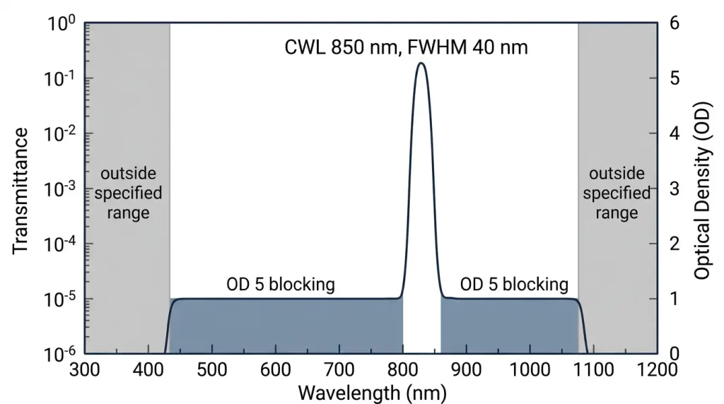
To specify the OD blocking range for a bandpass filter you need two independent numbers, not one: the depth of rejection, given as optical density (OD), and the wavelength interval over which that rejection is guaranteed. The interval is set by your system rather than by the filter. It has to cover every wavelength where your source emits and your detector responds, plus margin for angle-of-incidence shift and manufacturing tolerance. The OD value follows from the signal-to-background ratio your measurement needs, and that ratio depends on light integrated across the entire blocked band, not on the single worst wavelength.
Get either number wrong and the filter will pass its incoming inspection while your instrument fails its noise floor.
What OD and blocking range mean on a datasheet
Optical density is defined as OD = −log₁₀(T), where T is transmittance expressed as a fraction between 0 and 1. It is a logarithmic convenience for describing very small transmittance values, nothing more.
| OD | Transmittance (T) | Transmittance (%) | Attenuation factor |
|---|---|---|---|
| 2 | 10⁻² | 1% | 100× |
| 3 | 10⁻³ | 0.1% | 1,000× |
| 4 | 10⁻⁴ | 0.01% | 10,000× |
| 5 | 10⁻⁵ | 0.001% | 100,000× |
| 6 | 10⁻⁶ | 0.0001% | 1,000,000× |
| 8 | 10⁻⁸ | 0.000001% | 100,000,000× |
The blocking range is the wavelength interval over which the stated OD applies. A specification reading “OD ≥ 5, 300 nm to 1150 nm” means nothing outside 300 to 1150 nm is controlled. Below 300 nm and above 1150 nm the filter may transmit freely, and often does.
Two conventions exist for how the OD applies inside that interval, and they are not equivalent. Absolute blocking means no wavelength in the range exceeds the stated transmittance. Average blocking means the transmittance averaged over the range does not exceed it, which permits narrow leakage spikes well above the nominal level. Several major filter suppliers quote average blocking over defined intervals as their standard. Always state which one you are buying.
Why a bandpass filter needs separate blocking at all
A thin-film bandpass filter is a Fabry-Perot cavity, or a series of coupled cavities, formed by two quarter-wave dielectric mirror stacks separated by a spacer layer. The mirror stacks reject light only inside their high-reflectance zone, and that zone is narrow. For a quarter-wave stack the fractional width of the stopband is
Δg = (2/π) · arcsin[(n_H − n_L)/(n_H + n_L)]
where g = λ₀/λ is the normalized frequency and n_H, n_L are the high and low refractive indices of the layer pair.
Run the numbers for a common hard-coating pair, tantalum pentoxide (Ta₂O₅, n ≈ 2.10 in the visible) and silicon dioxide (SiO₂, n ≈ 1.46). Δg comes out near 0.115. Centered at 550 nm, the stack reflects strongly only from roughly 520 nm to 584 nm. That is about 64 nm of intrinsic rejection from a coating that has to hide a passband from a silicon detector sensitive across 750 nm of spectrum.
Everything outside that zone is transmitted by the interference structure, and the substrate transmits too. Fused silica is clear from below 200 nm to beyond 2 µm. So blocking over a useful range is always a deliberate addition: more stack pairs at staggered reference wavelengths, a stacked longpass and shortpass pair, an absorbing glass substrate, or a combination. Each addition costs transmission, thickness, and money. This is why the blocking range is the single most expensive line on a bandpass filter specification.
Setting the blocking range: where source and detector overlap
The correct blocking range is the intersection of two spectra: what your source can emit and what your detector can convert into signal. Light outside either range is harmless. Light inside both, at any wavelength, becomes background.
This is why the same filter can be excellent in one instrument and useless in another. A 340 nm bandpass filter working with a deuterium source and a bialkali photomultiplier tube (PMT) sees a shared response window only a few hundred nanometers wide. Move that same filter into a system with a tungsten-halogen lamp and a silicon photodiode and the shared window stretches past 1100 nm, where the lamp puts out most of its power and the coating may have long since stopped blocking.
| Detector | Typical response range | Blocking range to consider |
|---|---|---|
| Bialkali PMT | ~300 to 650 nm | 200 to 700 nm |
| Multialkali PMT | ~300 to 900 nm | 200 to 950 nm |
| Silicon photodiode / CMOS | ~350 to 1100 nm | 300 to 1150 nm |
| InGaAs | ~900 to 1700 nm | 800 to 1750 nm |
| Extended InGaAs | ~1200 to 2600 nm | 1100 to 2650 nm |
| InSb | ~1 to 5.5 µm | 0.9 to 5.6 µm |
| Uncooled microbolometer | ~8 to 14 µm | 7 to 15 µm |
Ranges vary by device, window material, and cooling, so read the responsivity curve for the part you are actually buying. Note where responsivity becomes negligible, not where the datasheet stops plotting.
Then extend the interval. A blocking edge that stops exactly at the detector cutoff leaves nothing for angle shift, deposition tolerance, or thermal drift. Roughly 50 nm of margin past the point where responsivity falls to a negligible level is a defensible starting position in the visible and near-infrared.
How deep the OD needs to be
The quantity that determines your measurement floor is not the OD at the worst wavelength. It is the total leaked flux reaching the detector, integrated over the blocking range and weighted by the source spectrum and detector responsivity:
Signal / Background = ∫_passband Φ(λ)·R(λ)·T(λ) dλ ⁄ ∫_blocked Φ(λ)·R(λ)·T_block(λ) dλ
where Φ(λ) is source spectral flux, R(λ) is detector responsivity, and T(λ) is filter transmittance. Manufacturers sometimes call the result integrated blocking or filter signal-to-noise ratio, and it is always system-dependent.
The practical consequence is that a wide blocking band buys you less than the OD number suggests. Take a 10 nm FWHM passband at 90% transmission, with OD6 blocking held across 700 nm of detector response, and assume the out-of-band spectral flux is roughly equal to the in-band flux per nanometer. Signal scales as 10 × 0.9 = 9. Leakage scales as 700 × 10⁻⁶ = 7 × 10⁻⁴. The ratio is about 1.3 × 10⁴, so an OD6 filter delivers an effective integrated rejection near OD4 in that system.
Under a strong out-of-band source it gets worse. If the blocked flux is a hundred times the in-band flux, as it can be when a broadband lamp illuminates a narrow fluorescence emission band, that effective OD4 drops to OD2 and the background dominates the measurement.
Calculate integrated leakage with your real source spectrum before choosing an OD level. If the result demands much more than OD6 across a wide range, reduce the out-of-band flux at the source instead. An excitation cleanup filter, a baffle, or a narrower source is usually cheaper than two more OD of blocking.
Angle of incidence shifts the blocking edges too
Every wavelength feature of a thin-film filter moves toward the blue as the angle of incidence (AOI) increases:
λ(θ) = λ₀ · √(1 − (sin θ / n_eff)²)
with n_eff the effective index of the coating, typically between about 1.5 and 2.5 depending on the material pair and cavity design. Higher n_eff means less shift.
For n_eff = 1.85 at θ = 15°, the shift factor is 0.990, so an 850 nm center wavelength (CWL) moves to about 842 nm. The blocking band edges move by the same fraction. Designers routinely account for the passband shift and forget the blocking edges, which is a mistake, because the transition zone adjacent to the passband is exactly where out-of-band light is most likely to be intense.
Two further effects matter. In a converging beam every ray angle is present at once, so the blocking edge nearest the passband softens rather than translating cleanly. Above roughly 10° to 15°, s-polarized and p-polarized light acquire different effective indices and shift by different amounts, broadening the transition regions further. Specify AOI as a range, for example 0° to 12° half-angle, not as a single nominal value.
Comparing blocking technologies
| Approach | Typical achievable OD | Blocking range | Passband transmission | Durability | Relative cost |
|---|---|---|---|---|---|
| Hard-coated all-dielectric, single substrate (ion-assisted deposition or plasma sputtering) | OD 4 to 6, higher with more layers | Wide, set by number of stacks; hundreds of layers common | High, often above 90% | Excellent; dense, non-hygroscopic | Moderate to high |
| Hard-coated, two components cemented or air-spaced | OD 6 to 8+ | Very wide | Lower; losses multiply | Excellent | High |
| Evaporated soft coating plus colored-glass absorber | OD 4 to 5 typical | Wide where the glass absorbs, poor where it does not | Moderate; glass absorption cuts peak T | Sensitive to humidity; usually sealed or laminated | Low to moderate |
| Metal-dielectric / induced transmission | Broad, deep rejection extending far into the IR | Very wide | Low, often well under 50% | Good | Moderate |
Hard-coated all-dielectric filters have displaced soft-coated designs in most visible and near-infrared instruments because they hold transmission and survive humidity. Soft-coated constructions still earn their place in the ultraviolet and where a colored glass happens to absorb precisely where you need blocking.
When requesting a quote from a filter supplier such as GIAI Photonics, send the source spectrum and detector responsivity curve along with the CWL and FWHM. That information determines the blocking construction, and without it the supplier has to guess conservatively, which raises price.
What you give up when you push blocking harder
Deeper and wider blocking means more layers. More layers means:
- Lower peak transmission. Every additional interface adds scatter and absorption loss. Pushing from OD4 to OD6 across a wide range commonly costs several percentage points of peak transmission.
- Higher coating stress and worse surface figure. Thick multilayer stacks bow the substrate, and on a thin window this can dominate transmitted wavefront error. If wavefront matters, specify substrate thickness and transmitted wavefront together.
- More passband ripple. Multi-cavity designs with heavy blocking often show structure across the passband that a single FWHM number hides. Ask for the full transmission curve.
- Longer lead time and higher price. Deposition run time scales with layer count, and yield falls as tolerances tighten.
Narrowing FWHM while holding blocking constant carries its own penalty: peak transmission drops, CWL tolerance becomes a larger fraction of the bandwidth, and the filter grows far more sensitive to AOI and temperature.
Common specification mistakes
Blocking range narrower than detector response. A 905 nm LiDAR (light detection and ranging) receiver filter blocked from 400 to 1000 nm still lets solar radiation at 1020 nm through onto a silicon avalanche photodiode that responds there. Specify to the detector’s real cutoff plus margin.
Assuming the substrate blocks where the coating does not. Colored absorbing glasses commonly become transparent again in the near-infrared. A blue-glass-based design that blocks beautifully across the visible can be nearly clear at 900 nm, exactly where a silicon sensor is still sensitive.
Confusing average with absolute blocking. An average OD5 specification can permit a narrow spike at OD3. If your out-of-band source is a laser line, that spike is the only wavelength that matters.
No margin at the near-band blocking edge. The blocking edge adjacent to the passband must clear the passband by the AOI shift plus the CWL manufacturing tolerance plus thermal drift. Specifying blocking that starts 5 nm from the passband edge on a filter used at 12° AOI usually produces leakage on delivery.
Buying OD6 and mounting it in an OD3 housing. Light that bypasses the filter through a mount gap, or scatters off a bore wall, does not care about the coating. A 0.1% geometric leak path around the filter caps your system at OD3 regardless of the part number. Verify blocking at system level, in the housing, with the real source.
Specifying deeper OD than anyone can measure. Commercial spectrophotometers are noise-limited well before OD8 across a wide range, and the practical floor is worse in the ultraviolet and beyond about 1500 nm. If you specify OD8, ask how it will be verified. The honest answer is often a laser-based measurement at discrete wavelengths, a modeled value, or a system-level test.
How to specify OD blocking range for a bandpass filter on a drawing
Write the blocking as a set of intervals with an explicit convention and explicit exclusions. A workable template:
Bandpass filter, hard-coated, all-dielectric

CWL:            850.0 nm ± 2.0 nm, at 0° AOI, 23 °C
FWHM:           40 nm ± 8 nm
Transmission:   Tavg ≥ 90% over CWL ± 20 nm
Blocking:       OD ≥ 5 absolute (T ≤ 1 × 10⁻⁵), 300 nm to 1150 nm,
                excluding 820 nm to 880 nm
                OD ≥ 3 absolute, 1150 nm to 1200 nm
AOI:            0° to 12° half-angle, unpolarized
Operating temp: 0 °C to 50 °C
Clear aperture: ≥ 90% of diameter
Surface quality:60-40 scratch-dig per MIL-PRF-13830B
                (or per ISO 10110-7 if the drawing set uses ISO)
Durability:     Adhesion, humidity, moderate abrasion per MIL-C-48497A
Measurement:    State method and noise floor for each blocking interval
State the AOI and temperature the CWL is referenced to. Without them, the center wavelength number is ambiguous and disputes at incoming inspection become unresolvable.
Frequently asked questions
Is OD6 always better than OD4? Only if you need it. OD6 across a wide range adds layers, which lowers peak transmission, increases coating stress and cost, and may not be verifiable by standard measurement. Calculate integrated leakage using your source spectrum first. Many machine vision and general instrumentation systems perform identically with OD4 and a well-baffled housing.
What blocking range should I specify if I do not know the source spectrum? Default to the detector’s full response range plus roughly 50 nm of margin at each end. This is the conservative choice and it is what a supplier will assume anyway. If you later characterize the source and find its emission is narrow, you can often relax the range and recover transmission or cost.
Why does my filter measure only OD5 when the datasheet says OD6? Most likely you are seeing the instrument’s noise floor rather than the filter. Broadband spectrophotometers are noise-limited near OD5 to OD6 across much of the visible and near-infrared, and worse in the ultraviolet and beyond 1500 nm. Stray light inside the instrument produces the same artifact. Ask the supplier for the measurement noise floor at each wavelength band.
Can I stack two filters to reach deeper blocking? Roughly yes: optical densities add, so OD4 plus OD4 approaches OD8. Three cautions. The passbands must overlap after accounting for the CWL tolerance of both parts, transmission losses multiply, and the air gap between two parallel filters creates an etalon and ghost reflections. Tilting one part slightly is the usual fix, but that shifts its spectrum.
Does blocking apply at all angles? No. The specification applies at the stated AOI. Blocking edges shift toward shorter wavelengths with angle by the same factor as the passband, and above about 10° to 15° the s and p polarizations separate. Specify the full angular cone your optical design delivers, including edge-of-field chief ray angles.
How does temperature affect blocking? Refractive index and layer thickness both change with temperature, shifting the whole spectrum. Hard-coated filters drift far less than soft-coated ones, and in most room-temperature instruments the effect is small next to the AOI shift. In outdoor or thermally cycled equipment, request the temperature coefficient and include it in your near-band margin.
Blocking range is a system specification wearing a component’s clothing, so define it from your source and detector before you compare parts. GIAI Photonics supplies bandpass, narrow bandpass, longpass, shortpass, notch, and infrared filters along with custom optical coatings for applications where the blocking requirement is set by the instrument rather than the catalog.