
Technical Resources
How Coating Materials Are Selected for a Wavelength Range
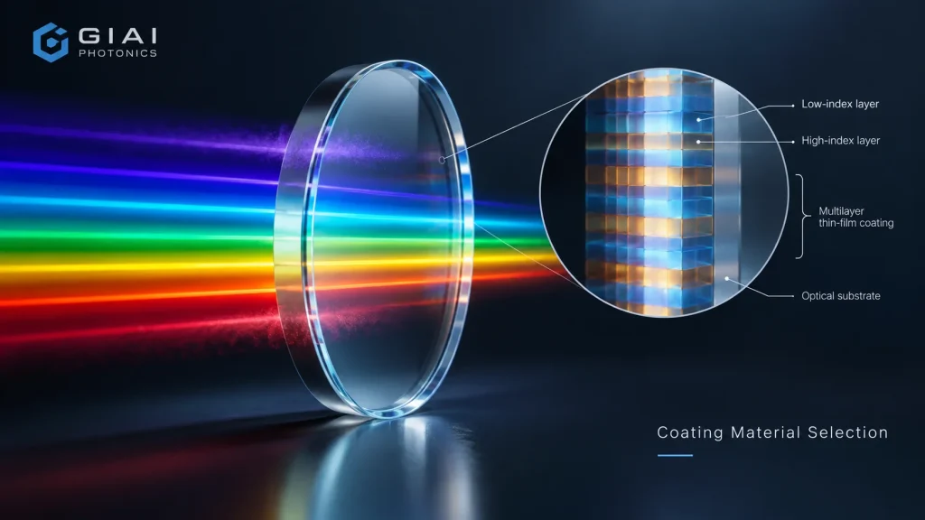
How are coating materials selected for a wavelength range? Engineers first find materials that are transparent across every wavelength where the coating must transmit or reflect light, then choose a high-index/low-index pair whose index contrast gives enough bandwidth with a practical number of layers. The shortlist is then narrowed by laser damage threshold, film stress, environmental stability, substrate compatibility and deposition process.
Coating material selection is the step that decides whether a multilayer design can work at all. A design program can return an excellent theoretical curve for almost any target, but the curve is only meaningful if every layer material has low absorption at the operating wavelengths and can be deposited reproducibly on the intended substrate. That is why a TiO₂/SiO₂ stack that works well in the visible band is unsuitable for a 266 nm laser mirror, and why an LWIR anti-reflection coating on germanium uses a completely different material family.
This guide explains how thin-film coating materials are selected for a wavelength range, which physical limits set each material’s usable window, and how index contrast, laser damage, stress and process choice change the answer from the deep UV to the long-wave infrared.
Coating Material Selection for a Wavelength Range: The Short Method
In practice, material selection follows a fixed order. Each step removes candidates, so the sequence matters more than any single parameter.
- Define the full spectral range the coating must handle — not only the passband, but also the reflection band, the blocking range that matters to the detector, any laser lines, and the wavelength shift caused by the real angle of incidence (AOI).
- Remove materials that absorb inside that range. The short-wavelength limit is set mainly by the material’s band gap; the long-wavelength limit by vibrational (multiphonon) absorption and absorbed water.
- Choose a high-index / low-index pair with enough index contrast for the required bandwidth, steepness and reflectance, without an impractical layer count.
- Check power handling. For laser optics, wider band-gap materials and field-aware designs usually give more damage margin.
- Check mechanics and environment — film stress, total thickness, adhesion, moisture sensitivity and operating temperature.
- Confirm substrate and process compatibility — substrate transmission range, thermal expansion, allowed deposition temperature, and whether evaporation, ion-assisted deposition or sputtering will be used.
Step 1: Define the Real Spectral Range Before Choosing Materials
The most common selection error is to choose materials for the nominal design wavelength only. A coating material must be transparent wherever light carries meaningful energy through the layers. For an interference filter, that usually includes the passband, the edges, and the reflection zones used for blocking. For a dichroic beamsplitter, it includes both the transmitted and the reflected channel.
Three practical points often enlarge the range:
- AOI shift. Interference features move toward shorter wavelengths as AOI increases. For a single-cavity bandpass filter the shift is commonly approximated by λ(θ) = λ₀ · √(1 − (sin θ / neff)²), where neff depends on the layer materials and design. If the system uses a converging beam or tilted mounting, the materials must remain transparent over the shifted band as well. See how polarization affects optical filter spectra at oblique incidence.
- Source and detector response. A silicon detector responds to roughly 1.1 µm; an InGaAs or thermal detector extends much further. Energy outside the passband that the detector can see must be blocked, and the blocking design itself places light inside the layers.
- Absorption outside the useful band is not always a problem. Light that is strongly reflected by the outer layers barely penetrates the stack, and some absorbing glass substrates are deliberately used for blocking. The requirement is transparency where the design depends on low loss — not across the whole spectrum.
Why Every Coating Material Has a Usable Wavelength Window
Dielectric coating materials are transparent between two absorption regions. On the short-wavelength side, photons with energy above the band gap are absorbed; high-index oxides such as TiO₂ have a smaller band gap than SiO₂, so their absorption edge sits at a longer wavelength. On the long-wavelength side, lattice vibrations absorb infrared light, and porous films can show additional absorption bands from trapped water. Material suppliers report water bands in pure fluoride films near 2.9 µm and 6.1 µm, which become weaker at higher substrate temperature.
The edge is not a step function. Absorption rises gradually as the wavelength approaches the edge, and the extinction coefficient of a thin film depends strongly on stoichiometry, density and deposition conditions. A useful working rule is to keep the operating wavelength well away from the listed edge, especially for high-power or high-reflectance designs where small absorption accumulates over many layers.
Common Thin-Film Coating Materials by Wavelength Range
The table summarizes typical properties reported by coating-material suppliers and reference tables. Treat the values as starting points for selection, not as specifications: thin-film refractive index commonly varies by several percent with deposition method, and the long-wavelength end of oxide ranges applies to thin layers. One supplier notes that oxides are generally useful below about 7 µm, with fluorides, ZnS, ZnSe and Ge used beyond that.
| Material | Typical role | Approx. film index | Approx. transparent range (film) | Selection notes |
|---|---|---|---|---|
| MgF₂ | Low index; single-layer AR | ~1.38 @ 550 nm | VUV to ~6 µm | Very low index and deep-UV transparency; tensile stress; good density usually needs a heated substrate |
| SiO₂ | Standard low index, UV–NIR | ~1.46 @ 550 nm | ~0.2 to ~7 µm (thin layers) | Hard, stable partner for most oxide stacks; strong Si–O absorption near 9 µm rules it out for LWIR |
| Al₂O₃ | Medium index; UV partner | ~1.60–1.68 @ 550 nm | >190 nm to ~7 µm | Used with SiO₂ or fluorides in DUV/UV designs where higher-index oxides absorb |
| HfO₂ | High index for UV and laser optics | ~1.90–2.07 @ 550 nm | ~230 nm to ~8 µm | Wider band gap than Ta₂O₅ or TiO₂; common choice for UV and high-power laser coatings |
| Ta₂O₅ | High index, VIS–NIR | ~2.07–2.18 @ 550 nm | ~300 nm to ~10 µm | Good balance of index, absorption and stability for NIR laser and filter coatings |
| Nb₂O₅ | High index, VIS–NIR | ~2.27–2.33 @ 550 nm | ~380 nm to ~8 µm | Higher index than Ta₂O₅; absorption edge closer to the visible |
| TiO₂ | Highest-index common oxide | ~2.07–2.50 @ 550 nm | ~400 nm to IR (thin layers) | Maximum contrast with SiO₂ in VIS–NIR; index strongly process-dependent; lowest band gap of the group |
| YF₃ / YbF₃ | Low index, MWIR–LWIR | ~1.3–1.4 @ 10 µm | ~0.2 to ~12 µm | Non-radioactive replacements for ThF₄ in LWIR; columnar growth and tensile stress need control |
| ZnS | Medium/high index, VIS–LWIR | ~2.0–2.15 @ 10 µm | ~0.4 to ~14 µm | Classic IR partner for Ge or fluorides; compressive stress partly offsets tensile fluorides |
| ZnSe | High index, IR | ~2.35 @ 5–10 µm | ~0.6 to ~16 µm | IR coating material and substrate; check compatibility with the full stack |
| Si | High index, SWIR–MWIR | ~3.4 @ 3 µm | ~1 to ~8 µm | Very high contrast against oxides in the NIR–MWIR |
| Ge | Highest index, MWIR–LWIR | ~4.0–4.1 @ 10 µm | ~1.7 µm to beyond 12 µm | Highest index contrast in the IR; absorption rises with temperature; adhesion with fluorides may need a bonding layer |
Approximate published supplier/reference data; ranges and indices are process-dependent and are not GIAI product specifications.
Index Contrast: Why the Material Pair Decides Bandwidth and Layer Count
Once the transparent candidates are known, the pairing decision is driven by the ratio nH/nL. For an ideal quarter-wave stack at normal incidence, the full width of the high-reflectance zone, expressed in relative wavenumber g = λ₀/λ, is:
Δg = (4/π) · arcsin[(nH − nL) / (nH + nL)]
A larger contrast widens the reflection band and reaches a target reflectance with fewer layers. The worked examples below use representative film indices for ideal, lossless stacks; real designs add matching layers, absorption and process variation.
| Example pair (illustrative) | Center λ₀ | nH / nL used | Approx. reflection band | Quarter-wave layers for ≥99.9% R (ideal) |
|---|---|---|---|---|
| TiO₂ / SiO₂ on glass | 550 nm | 2.35 / 1.46 | ~478–647 nm (~170 nm) | 17 |
| Ta₂O₅ / SiO₂ on fused silica | 1064 nm | 2.07 / 1.44 | ~954–1202 nm (~250 nm) | 21 |
| HfO₂ / SiO₂ on fused silica | 355 nm | 2.05 / 1.48 | ~322–396 nm (~74 nm) | 25 |
| Ge / ZnS on Ge | 10 µm | 4.0 / 2.1 | ~8.3–12.5 µm (~4.2 µm) | 13 |
Calculated from the stopband equation above and the standard quarter-wave stack reflectance formula; incident medium air, normal incidence, no absorption. Illustrative only.
The UV row shows the central trade-off. Moving to shorter wavelengths forces engineers away from high-index, small-band-gap oxides, so the available contrast drops. The result is a narrower reflection band and more layers for the same reflectance — and each extra layer adds absorption, scatter, stress and thickness error. The same logic applies to edge steepness and blocking width in filters: lower contrast generally means more layers. Contrast also affects angular sensitivity, because a higher effective index tends to reduce the AOI-induced shift of interference features.
Anti-reflection coatings follow a different rule
For AR coatings, the target is index matching rather than maximum contrast. A single quarter-wave layer gives zero reflection at one wavelength only if its index equals √(n0·ns). For a glass substrate with ns = 1.52, the ideal value is about 1.23, lower than any durable common material. MgF₂ (n ≈ 1.38) therefore leaves about 1.3% reflection per surface at the design wavelength, compared with about 4.3% for uncoated glass. On fused silica (n ≈ 1.46) the same layer leaves about 1.7%, while on sapphire (n ≈ 1.77) it falls to about 0.1%. Lower residual reflection or broader bandwidth requires multilayer AR designs with additional materials, as discussed in V-coat vs broadband AR coating.
How Material Choices Change Across Wavelength Regions
Deep UV and UV (below about 400 nm)
Absorption is the controlling constraint. TiO₂ and Nb₂O₅ are normally excluded; Ta₂O₅ becomes absorbing toward 300 nm; HfO₂ extends usable high-index performance to about 230 nm. At excimer wavelengths such as 193 nm, designs typically rely on Al₂O₃ and SiO₂ or fluorides such as MgF₂ and LaF₃, where scatter and absorption losses become as important as index. Substrates must also transmit the band, which usually means UV-grade fused silica, CaF₂ or MgF₂ rather than standard optical glass.
Visible and near infrared (about 400 nm to 1.1 µm)
This is the most flexible region. SiO₂ is the usual low-index material, paired with TiO₂, Nb₂O₅ or Ta₂O₅ depending on how much contrast, absorption margin and stability the design needs. Machine-vision bandpass filters, dichroic mirrors and NIR laser mirrors are commonly built from these oxide pairs. For blue and violet bands near 400 nm, the absorption edge of TiO₂ and Nb₂O₅ deserves an explicit check.
SWIR (about 1.1–3 µm)
Oxide pairs remain usable, and silicon becomes an option as a very high-index layer above roughly 1.1 µm. Two details often matter: thicker layers (because physical thickness scales with wavelength) and water absorption near 2.7–3 µm in porous films. Denser films from ion-assisted or sputtered processes reduce moisture-related shift and absorption; see IBS vs IAD optical coating.
MWIR (about 3–5 µm)
Some oxides, Si, Ge, ZnS and fluorides are all candidates, so selection depends on substrate (Si, sapphire, CaF₂, Ge or ZnSe), durability and residual moisture bands. Designs near 3 µm should be checked for water absorption in fluoride or porous oxide layers.
LWIR (about 8–12 µm)
Oxides are generally avoided, and SiO₂ in particular absorbs strongly near 9 µm. Typical LWIR stacks use Ge as the high-index material, ZnS or ZnSe as a medium-index material, and fluorides such as YF₃ or YbF₃ as the low-index material. ThF₄ was historically used as the low-index partner but is radioactive, and non-radioactive alternatives are now used. Because a quarter-wave layer at 10 µm is roughly 0.6 µm thick in Ge and about 1.9 µm thick in a fluoride with n ≈ 1.35 (versus about 94 nm for SiO₂ at 550 nm), LWIR stacks can reach several micrometers of total thickness, making stress and adhesion central selection criteria. For substrate choices in this band, see germanium vs ZnSe infrared windows and the optical vs physical thickness explanation.
Metal layers for broadband reflection
When a mirror must reflect across a very wide range, metals are selected by wavelength in the same way: aluminum for UV through IR, silver from roughly 400 nm upward, and gold mainly in the red and infrared. Protective and enhancing dielectric overcoats then have to satisfy the same transparency rules. Related comparisons: dielectric vs metallic coating and protected vs enhanced aluminum.
Beyond Transparency: Other Factors That Narrow the Shortlist
| Factor | Why it matters for material choice | Typical consequence |
|---|---|---|
| Laser damage threshold | For short pulses, damage threshold has been shown to scale with band gap; for longer pulses, defects and absorption often dominate | Wider band-gap high-index layers (e.g., HfO₂) or mixtures are preferred over TiO₂ in demanding laser coatings; see what determines coating LIDT |
| Film stress and total thickness | Tensile fluorides and compressive ZnS or sputtered oxides change substrate shape and adhesion | Thick IR stacks and long-pass/broadband filters need stress-balanced material combinations |
| Density and moisture | Porous films adsorb water, which shifts spectra and adds IR absorption bands | Process choice (heated evaporation, IAD, sputtering) can matter as much as material choice |
| Substrate compatibility | Substrate must transmit the band, tolerate the deposition temperature and roughly match thermal expansion | Temperature-sensitive or cemented parts may exclude hot-deposited MgF₂ |
| Environmental exposure | Humidity, abrasion, cleaning and temperature cycling attack softer or hygroscopic layers | Durable outer layers or hard coatings for exposed surfaces; see hard vs soft coated filters |
| Temperature in operation | Some materials change index or absorption with temperature (Ge absorption increases as it heats) | Check spectral shift and absorption at the real operating temperature |
Common Mistakes in Coating Material Selection
- Selecting by design wavelength only while ignoring blocking zones, AOI shift or the detector’s full response.
- Using bulk refractive index values for thin-film design. Film index depends on process and density.
- Operating near an absorption edge, e.g., TiO₂ or Nb₂O₅ in a violet design, or porous fluorides near 3 µm.
- Maximizing index contrast without checking LIDT or stress. The highest-index material is not automatically the best choice.
- Treating the substrate as neutral. Substrate transmission, temperature limit and expansion often decide which coating materials are allowed.
- Accepting a curve without test conditions. A spectrum without AOI, polarization and wavelength range does not prove the coating fits the system.
How to Verify That the Material Choice Works
Material selection is confirmed by measurement, not by the design curve alone. Typical verification, chosen according to the project specification, includes:
- Spectral transmission and reflection over the full required range at the specified AOI and polarization, using a spectrophotometer for UV–NIR or FTIR for infrared.
- Absorption and loss checks for UV, high-reflectance and laser coatings, since T + R alone may hide small losses that matter at high power. Background: how material absorption affects optical transmission.
- Environmental and durability tests (adhesion, abrasion, humidity, temperature) when the operating environment requires them, followed by a repeat spectral check.
- Laser damage testing to the relevant pulse length, wavelength and spot size when LIDT is specified; the ISO 21254 series defines common test methods.
What to Specify When Requesting a Custom Coating
Supplying the following information lets a coating engineer select materials against the real application instead of a nominal wavelength:
- Full wavelength range: passband, reflection band, blocking range and any laser lines
- Required T, R or OD values and the wavelengths where they apply
- AOI (including cone angle) and polarization state
- Substrate material, dimensions, clear aperture and coated surfaces
- Laser parameters if relevant: wavelength, pulse duration, repetition rate, power or energy density
- Operating temperature, humidity, cleaning and environmental requirements
- Inspection criteria, test conditions and quantity
GIAI Photonics supports optical coatings on filters, lenses, mirrors, windows, prisms and beamsplitters as part of custom optics projects. For each project, GIAI reviews the drawing, sample, optical requirements, substrate, geometry, coating conditions and inspection criteria before defining the manufacturing route. More background is available in the Filters & Coatings resources and the custom optics process.
Planning a coating for a specific wavelength range? Send the drawing or sample with the wavelength range, substrate, AOI, polarization, required T/R/OD, environment and inspection criteria to our engineering team for technical review.
FAQ
Why are TiO₂/SiO₂ coatings not used for UV laser optics?
TiO₂ has a relatively small band gap, and thin films begin absorbing toward about 400 nm. In UV designs that absorption causes transmission loss, heating and lower damage resistance. UV coatings therefore use wider band-gap materials such as HfO₂, Al₂O₃, SiO₂ or fluorides, accepting lower index contrast and more layers.
Is a higher refractive index material always better?
No. Higher contrast reduces layer count and widens reflection bands, but the highest-index materials usually have smaller band gaps, which narrows their UV transparency and tends to lower laser damage resistance. In the infrared, very high-index Ge also brings temperature-dependent absorption. The best material is the one that meets the spectral, power and environmental requirements together.
Can one set of coating materials cover both visible and infrared?
Only for limited ranges. Oxide pairs work well from the near UV to the SWIR and part of the MWIR, but they are generally not used for LWIR stacks. A coating spanning visible and LWIR is difficult because few materials are transparent across both regions, and the required layer thicknesses differ by more than an order of magnitude.
Does the deposition process change a material’s usable wavelength range?
It changes the practical range. Packing density, stoichiometry and moisture content affect refractive index, absorption near the edges and IR water bands. Ion-assisted deposition and sputtering usually produce denser films with less moisture-induced spectral shift than conventional evaporation, but they can also change stress. Material and process should be selected together.
Why do LWIR coatings use germanium, ZnS and fluorides?
Between 8 and 12 µm most oxides absorb, while Ge, ZnS, ZnSe and fluorides such as YF₃ or YbF₃ remain transparent. Ge provides very high index, ZnS a medium index with compressive stress, and fluorides the low index, so combinations of these materials can build AR, bandpass and edge filters for thermal imaging and CO₂ laser systems.
References
- H. A. Macleod, Thin-Film Optical Filters, CRC Press — quarter-wave stack theory and material discussion.
- Umicore, Oxide evaporation materials for precision optics, lasers and coatings (transparency ranges and indices of oxide films).
- Umicore, Infrared coating materials data (fluorides, ZnS, Ge, Si).
- Materion, IR Coating Designs and Applications (MWIR/LWIR materials, ThF₄ replacement, stress).
- Materion, Coatings for Short Pulse Duration Laser Optics (band gap and LIDT).
- M. Mero et al., “Scaling laws of femtosecond laser pulse induced breakdown in oxide films,” Physical Review B 71, 115109 (2005).
- ISO 21254 series, Lasers and laser-related equipment — Test methods for laser-induced damage threshold.