
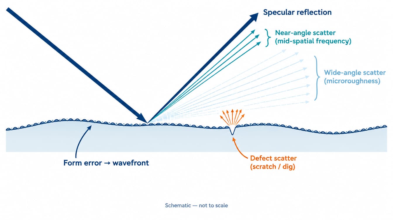
Mirror surface quality affects scatter through several different surface features. Microroughness sends a small fraction of the reflected light into a diffuse halo, and that fraction grows roughly with the square of rms roughness divided by wavelength. Scratches and digs scatter from discrete points. Coatings and contamination add their own roughness and particles. Flatness mostly distorts the reflected wavefront rather than scattering light out of the beam.
Scattered light causes two problems at once. It is light lost from the specular beam, which matters in laser cavities and low-loss systems. It is also light arriving where it is not wanted: veiling glare that lowers image contrast, or background in a Raman or fluorescence channel. Which surface feature dominates depends on the wavelength, the angle of incidence (AOI), the beam size and where the mirror sits in the optical system.
What “Surface Quality” Means for Mirror Scatter
On many drawings, “surface quality” means scratch-dig and nothing else. For scatter it is more useful to sort surface errors by their lateral size, because the spatial period of an error decides where the light goes.
| Surface feature | Lateral scale | Typical drawing callout | Effect on reflected light | Common measurement |
|---|---|---|---|---|
| Form (figure) error | Millimetres to full aperture | Flatness or irregularity (ISO 10110-5) | Aberrates the specular beam; very little light leaves it | Fizeau interferometer |
| Mid-spatial-frequency error | Roughly 0.1 mm to a few mm | Often not specified; a slope or PSD band when needed | Near-angle scatter: a halo close to the beam or image point | High-resolution interferometry, optical profiler |
| Microroughness | Below about 0.1 mm, down to the wavelength | Rq over a stated band, or a PSD (ISO 10110-8) | Wide-angle diffuse scatter | White-light interferometer, AFM, scatterometer |
| Scratches and digs | Isolated features, µm to mm | Scratch-dig (MIL-PRF-13830B) or ISO 10110-7 | Localized scatter and diffraction; possible laser damage sites | Visual or dark-field inspection, microscopy |
| Coating microstructure | nm to µm | Coating specification; rarely called out directly | Adds intrinsic roughness and interface scatter | Total or angle-resolved scatter on the coated part |
| Contamination | Particles and residue films | Cleanliness and handling requirement | Particle scatter, local absorption | Dark-field inspection, scatter measurement |
The boundaries between form, mid-spatial frequency and roughness vary between standards and suppliers. What matters is that a drawing states which band each requirement covers.
How Microroughness Creates Scatter
Every polished surface can be described as a sum of very shallow sinusoidal ripples. Each ripple acts like a weak diffraction grating and sends a little light out of the specular direction. For a surface whose rms roughness is much smaller than the wavelength, the fraction of reflected light scattered out of the specular beam is estimated by the total integrated scatter (TIS) relation of Davies and Bennett–Porteus:
Here σ is the rms roughness in the spatial-frequency band that actually scatters at this wavelength, θi is the angle of incidence and λ is the wavelength. The specular reflectance falls by about the same fraction: R ≈ R0 · exp[−(4πσ cos θi / λ)²], where R0 is the reflectance of an ideally smooth surface.
Three engineering consequences follow from this first-order model:
- Scatter scales with σ². Halving the relevant rms roughness cuts roughness scatter by about a factor of four.
- Scatter scales with 1/λ². The same mirror scatters about 9 times more at 355 nm than at 1064 nm, and about 100 times more at 1064 nm than at 10.6 µm.
- Oblique incidence reduces the roughness term by cos² θi. At 45° the model predicts half the normal-incidence value. Coating design and polarization also change scatter at oblique incidence, so this is a trend, not a correction factor.
The table below applies the model to a few roughness values. It is an illustrative calculation for a single smooth surface at normal incidence with R0 ≈ 1, not measured data for any product.
| Relevant rms roughness σ | 355 nm | 532 nm | 1064 nm | 10.6 µm |
|---|---|---|---|---|
| 0.5 nm | ≈ 310 ppm | ≈ 140 ppm | ≈ 35 ppm | ≈ 0.35 ppm |
| 1 nm | ≈ 1,250 ppm (0.13%) | ≈ 560 ppm | ≈ 140 ppm | ≈ 1.4 ppm |
| 2 nm | ≈ 5,000 ppm (0.50%) | ≈ 2,200 ppm (0.22%) | ≈ 560 ppm | ≈ 5.6 ppm |
Two conclusions are useful for budgeting. For UV mirrors and for cavities that count losses in ppm, sub-nanometre roughness matters. For a 10.6 µm mirror, a few nanometres of rms roughness produces very little scatter in absolute terms, so absorption, figure and coating durability are more often the limiting factors. Real coated mirrors can depart from these numbers, which is why critical parts are measured at the working wavelength.
Which Roughness Actually Scatters: Spatial Frequency and Scatter Angle
The period of a surface ripple sets the angle of the light it scatters. In the plane of incidence, the grating equation links them:
Here f is the spatial frequency (1 / period) and θs is the scatter angle. At normal incidence and 633 nm, a ripple period of about 36 µm scatters light at 1°, about 3.7 µm scatters at 10°, and about 0.73 µm scatters at 60°. Ripples shorter than the wavelength (f > 1/λ) cannot scatter into propagating directions, so they do not add to TIS at that wavelength.
In the smooth-surface Rayleigh–Rice theory, the angle-resolved scatter is proportional to the surface power spectral density (PSD) at the matching spatial frequency. The angular scatter pattern is therefore a map of the roughness spectrum, and a scatter measurement can be converted into band-limited roughness, and back.
This is why an Rq value without its bandwidth is incomplete. A white-light interferometer with a low-magnification objective and an AFM scanning 1 µm × 1 µm sample different spatial-frequency bands. They can report different Rq values for the same surface, and both can be correct. For scatter-critical mirrors, specify roughness over the band that maps to the angles your system cares about, specify a PSD limit, or specify scatter directly.
Periodic structures behave differently from random roughness. Diamond-turned metal mirrors carry tool marks with a nearly constant period d. Instead of a smooth halo, they send light into discrete diffraction orders at sin θ = mλ/d. These marks are often acceptable in the long-wave infrared. For visible and UV use, diamond-turned surfaces are commonly plated and polished to reduce this effect.

How Scratches and Digs Affect Mirror Scatter
Scratch-dig limits isolated cosmetic defects. It does not limit microroughness. Under MIL-PRF-13830B, the scratch number is a visual brightness grade compared with reference standards, not a width in microns. The dig number is the diameter of the largest dig in hundredths of a millimetre, so dig 10 means 0.10 mm. ISO 10110-7 grades imperfections by number and size and allows either a dimensional or a visibility method. A 10-5 surface can still carry nanometre-level roughness that scatters strongly in the UV. A super-polished surface can fail inspection because of one dig. The two specifications answer different questions, as explained in scratch-dig vs surface roughness.
How much a defect matters depends on how much of the beam it intercepts and where the mirror sits:
- Beam footprint. The same dig is a negligible fraction of a large collimated beam but a much larger fraction of a small beam near a focus.
- Position in the system. Defects near a pupil add a diffuse background across the field. Defects near an image or focal plane can be imaged as visible artifacts.
- Laser loading. Scratches, digs and embedded polishing residue can absorb or concentrate the field. Sites that scatter are often the same sites where laser damage starts; see what determines the laser damage threshold of a coating.
Tie the surface imperfection grade to the clear aperture, and state it if one zone, such as the beam footprint, needs a tighter grade than the rest of the surface.
How Coatings and Contamination Change Mirror Scatter
A thin-film coating largely replicates the substrate roughness beneath it. It also adds intrinsic roughness from film growth, and roughness can increase through a thick stack. In practice, a coating rarely makes a rough substrate smoother, so substrate polish sets the floor for the finished mirror.
- Deposition process. Dense films from energetic processes generally show less columnar microstructure than conventional evaporated films. Process selection is discussed in IBS vs IAD optical coating.
- Dielectric multilayers. Every interface scatters, and the scattered fields from partly correlated interfaces interfere. Near the centre of the reflection band, scatter often follows the single-surface trend. Near the band edges, scatter can rise sharply. Measure at the working wavelength and AOI rather than at a convenient test wavelength.
- Metal films. Silver, aluminum and gold films have a grain structure that adds roughness, and protective overcoats add interfaces. Their absorption loss is a separate term from scatter; see metallic mirror vs dielectric mirror.
Contamination often dominates scatter once a well-polished mirror is installed. Particles, cleaning residue and fingerprints all scatter, and some absorb. Cleaning can also introduce new scratches. Handling, packaging and cleaning procedures therefore belong in the specification for scatter-critical mirrors, not only in the assembly instructions.
Common Mistakes When Specifying Low-Scatter Mirrors
- Using scratch-dig as the scatter specification. It controls cosmetic defects, not the roughness that produces diffuse scatter.
- Treating flatness as a scatter number. A λ/10 flatness requirement controls low-spatial-frequency form error and the reflected wavefront, not microroughness; see surface flatness vs wavefront error.
- Quoting Rq without bandwidth. Without the instrument, objective or scan size, and filtering, two Rq values cannot be compared.
- Moving a visible-light specification into the UV. Because of the 1/λ² scaling, a roughness that is acceptable at 1064 nm may be several times too high at 355 nm.
- Measuring the bare substrate and assuming the coated part matches. Coating roughness and interface scatter add to the substrate contribution.
- Testing at the wrong geometry. Scatter measured at normal incidence and one wavelength may not represent a 45° fold mirror used at another wavelength.
- Over-specifying. Super-polishing an LWIR mirror where scatter is not the limiting term adds cost and lead time without improving the system.
How to Specify Mirror Surface Quality for a Scatter Budget
- Start from the system. Decide how much scattered or lost light is acceptable, and at which detector or field position it causes harm.
- Identify the critical angles. A halo close to the beam or image points to mid-spatial-frequency error. A raised background across the detector points to microroughness and particles.
- Write the requirement in the right form. Use Rq over a stated spatial-frequency band, a PSD limit, or a direct TIS or BRDF limit at the working wavelength and AOI.
- Add the defect requirement. State scratch-dig or ISO 10110-7 grades within the clear aperture, with a tighter zone if the beam footprint is small.
- Define the coating and how it is verified. State whether acceptance is measured on the part or on a coating witness sample, and remember that a witness sample may not share the part’s substrate polish.
- Include cleanliness, handling and packaging when the system is scatter-limited.
| Application | Main scatter concern | What to specify |
|---|---|---|
| Laser cavities and low-loss resonators | Total loss in ppm | TIS (with absorption) at the working wavelength and AOI; relevant roughness; coating process |
| Imaging and camera fold mirrors | Contrast loss and veiling glare | Microroughness band, scratch-dig in the clear aperture, cleanliness |
| Raman, fluorescence and spectroscopy | Background at the detection wavelength | Angle-resolved scatter at the excitation wavelength; pair with filter blocking |
| High-power laser delivery | Local scatter and damage initiation | Defect grade in the beam footprint, cleanliness, LIDT at stated test conditions |
| UV systems | 1/λ² growth of scatter | Tighter relevant roughness, verified at or near the UV wavelength |
| LWIR (for example 10.6 µm) | Usually small roughness scatter | Figure, absorption and coating durability first; periodic marks on diamond-turned parts |
In spectroscopy, mirror scatter and optical filters work together. A filter can remove scattered excitation light only when the scatter is at a different wavelength from the signal, as covered in how to reduce stray light with optical filters.
How to Verify Mirror Scatter
- Total scatter. An integrating sphere or Coblentz-sphere setup collects the light scattered outside a small cone around the specular beam and gives one TIS value per wavelength. ISO 13696 defines a test method for total scattering by coated and uncoated optical surfaces.
- Angle-resolved scatter. A goniometric scatterometer measures scatter versus angle (ARS or BSDF). ASTM E2387 describes standard practice for these measurements. The angular data can be converted into a PSD.
- Roughness. White-light interferometry and AFM measure surface height directly. Report the instrument, objective or scan size, sampling and filtering, and compare PSDs over overlapping bands.
- Surface imperfections. Visual inspection against comparison standards under defined illumination follows MIL-PRF-13830B. Dimensional assessment by microscope is one route under ISO 10110-7.
- Test as used. Where practical, measure the coated, cleaned part at the specified wavelength, AOI and polarization. Agree the test method and acceptance limits before production starts.
What to Send for a Low-Scatter Mirror RFQ
- Operating wavelength or band, AOI and polarization
- Beam diameter and whether the mirror sits near a pupil, a focus or an image plane
- Substrate, dimensions, clear aperture and flatness or wavefront requirement
- Roughness with its spatial-frequency band, or a TIS or BRDF limit with test conditions
- Surface imperfection grade (scratch-dig or ISO 10110-7) and any tighter zone
- Coating type, reflectance requirement and, for lasers, power level or LIDT test conditions
- Cleanliness, packaging and inspection report requirements, and expected quantity
GIAI Photonics reviews custom mirror projects against the drawing, sample, optical requirements, substrate, geometry, coating conditions and inspection criteria before defining the manufacturing route. When scatter is critical, agree the roughness band, defect grade and test conditions at the quotation stage, so acceptance is clear before polishing starts.
FAQ
Does a better scratch-dig specification reduce mirror scatter?
Only the scatter from isolated defects. Scratch-dig limits visible scratches and pits, but it does not control the nanometre-scale microroughness that produces diffuse wide-angle scatter. A 10-5 mirror can still scatter noticeably in the UV if its relevant rms roughness is high. If diffuse scatter matters, add a band-limited roughness, PSD or total scatter requirement alongside scratch-dig.
Which matters more for scatter: surface roughness or flatness?
For scatter, roughness usually matters more. Flatness describes low-spatial-frequency form error, which mainly aberrates the reflected wavefront and keeps light near the specular direction. Microroughness and mid-spatial-frequency errors send light out of the beam. A mirror can meet a tight flatness requirement and still scatter strongly if it is rough at micrometre scales.
Why does the same mirror scatter more in the UV?
In the smooth-surface model, total scatter scales with (σ/λ)². Shorter wavelengths make the same roughness look larger relative to the wavelength. They also make finer surface ripples able to scatter, because only spatial frequencies below 1/λ scatter into propagating directions. Moving from 1064 nm to 355 nm raises roughness scatter by about nine times.
Do metal mirrors scatter more than dielectric mirrors?
There is no general rule. Both replicate the substrate roughness. Metal films add grain roughness, while dielectric stacks add many scattering interfaces whose contributions interfere and can rise near the reflection band edges. The substrate polish, deposition process and working wavelength usually decide which mirror scatters less in a given system.
Can cleaning reduce mirror scatter?
Yes, when particles or residues are the main source, which is common for installed optics. Cleaning cannot remove roughness, scratches or digs, and poor technique can add scratches. For scatter-critical mirrors, define the cleaning method, handling and packaging, and inspect under dark-field illumination after cleaning.
Send the drawing or sample with the working wavelength, AOI, beam size, coating, roughness or scatter requirement and inspection criteria to the GIAI engineering team for technical review.